Polymer plane nano-channel production method

A production method and polymer technology, which are applied in the fields of micro-nanofluidic chip manufacturing, analytical chemistry, medicine, and life sciences, can solve the problems of complex process and long production cycle, and achieve simple production process, low cost and short cycle. Effect

Inactive Publication Date: 2009-07-08
DALIAN UNIV OF TECH
View PDF0 Cites 13 Cited by
  • Summary
  • Abstract
  • Description
  • Claims
  • Application Information

AI Technical Summary

Problems solved by technology

Laser or particle beam direct writing method requires expensive special equipment; nano hot pressing or hot pressing forming also needs special equipment, and also needs to make expensive pattern transfer template; sacrificial layer etching method requires relatively simple equipment, but often the process is complex, long production cycle

Method used


Image

  • Polymer plane nano-channel production method
  • Polymer plane nano-channel production method
  • Polymer plane nano-channel production method

Examples


Embodiment Construction

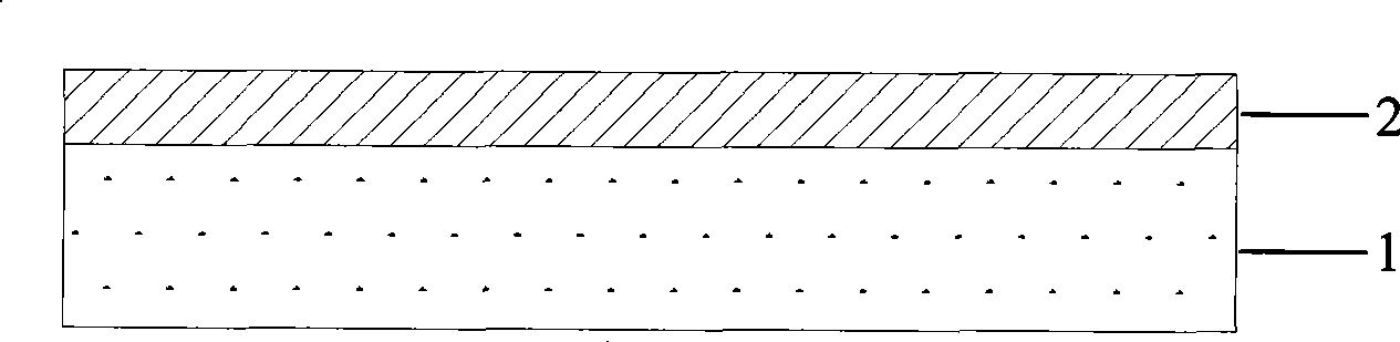
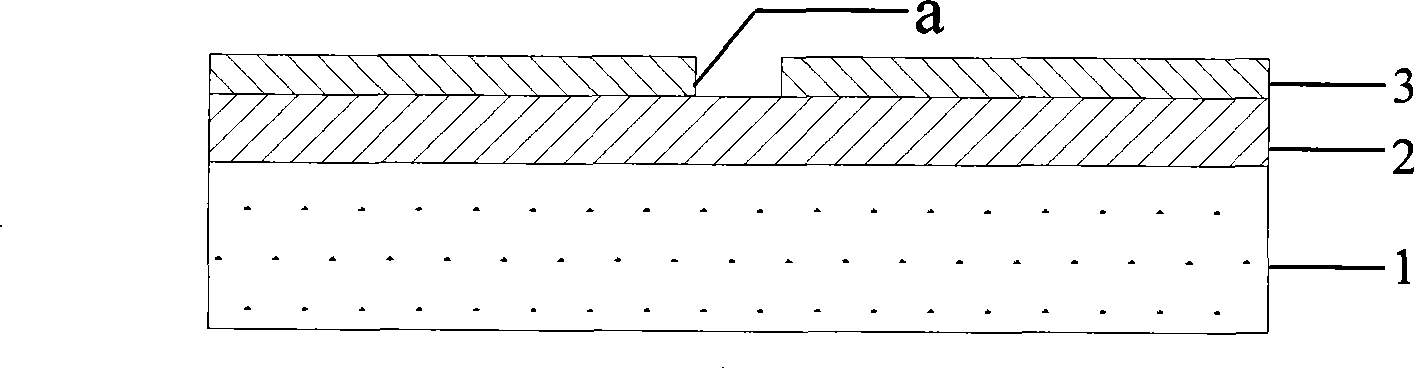
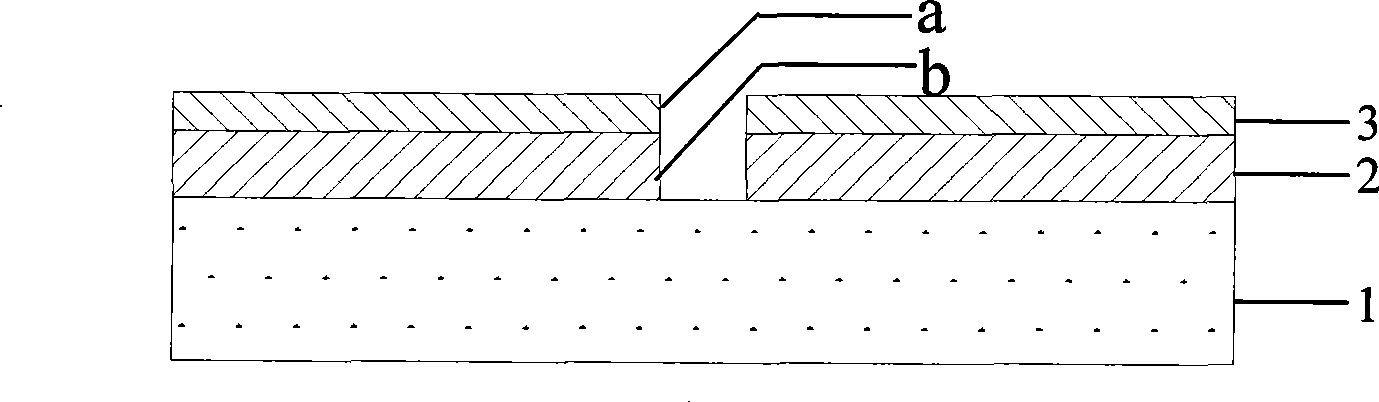
[0016] Embodiments of the present invention will be described in detail below in conjunction with technical solutions and drawings. as attached figure 1 , 2 , 3, 4, 5 and 6, a layer of copper with a thickness of about 80nm is sputtered on the polymer substrate 1 using the JS3X-80B magnetron sputtering station produced by Beijing Chuangweina Technology Co., Ltd. Film 2; adopt the model of Delta 80RC produced by SUSS MicroTec Company in Germany to spin-coat a layer of positive photoresist produced by AZ ElectronicMaterials Company on the surface of the copper film and be the positive photoresist of AZ MiR701. / min, and pre-bake on a hot plate at 55°C for 1 hour, then cover the mask plate on the photoresist 3, and use the UV photolithography machine model MA / BA6 produced by SUSS MicroTec, Germany, to photoresist 3 Expose for 30 seconds, put it into the developer solution for development, and obtain a photoresist pattern a with a width of micron order, and put it on a hot plate ...


PUM

PropertyMeasurementUnit
widthaaaaaaaaaa

Abstract

The invention relates to a making method of a polymer planar nano channel, which belongs to the technical field of making micro-nano flow-control chip and is used in the fields of life science, medicine, analytical chemistry, and the like. The making method comprises the following steps: firstly, making a metal masking figure with micron-sized line width on a polymer substrate on the basis of standard ultraviolet lithography and chemical wet method erosion technology; then, carrying out oxygen plasma etching on exposed polymer by means of a plasma cleaning machine and accurately controlling the etching depth of a polymer nano channel through setting etching time; and finally, removing the metal masking figure by means of chemical wet method erosion to obtain the polymer planar nano channel. The making method does not need to purchase reactive ion etching or inductive coupling plasma etching equipment with complex operation and high price in order to realize polymer etching. Moreover, the entire making process of the nano channel has simplicity, short cycle and low cost.

Description

technical field [0001] The invention belongs to the technical field of micro-nano fluidic chip manufacturing, and relates to a method for manufacturing a polymer planar nano-channel, which is applied in the fields of life science, medicine, analytical chemistry and the like. Background technique [0002] Micro-nanofluidic chip technology is one of the rapidly developing frontier fields of high-tech and interdisciplinary science and technology. It is an important technology platform for the development of life science, chemical science and information science in the future. The advantages of micro-nanofluidic chips in miniaturization, integration and portability provide a great opportunity for their applications in many fields such as biomedicine, drug synthesis and screening, environmental monitoring and protection, health and quarantine, judicial identification, and detection of biological warfare agents. a very broad prospect. Nano-channel fabrication technology is the ba...

Claims


Application Information

Patent Timeline
Patent Type & Authority Applications(China)
IPC IPC(8): G01N33/00G03F7/00
Inventor 刘军山乔红超刘冲徐征杜立群王立鼎
Owner DALIAN UNIV OF TECH
Why Eureka
Try Eureka