Process for preparing vertical structure phase-change memory

A technology of phase change memory and vertical structure, applied in static memory, digital memory information, information storage, etc., can solve the problems of complex process and high power consumption, and achieve the effect of simple process, reduced power consumption, and reduced power consumption

Inactive Publication Date: 2009-07-08
NANJING UNIV
View PDF2 Cites 7 Cited by
  • Summary
  • Abstract
  • Description
  • Claims
  • Application Information

AI Technical Summary

Problems solved by technology

[0003] The search found that the Chinese patent application with the application number 200510110783.X discloses a method for preparing phase-change memory device units using chalcogenide nanomaterials. The phase-change active layer used is a two-dimensional chalcogenide thin film, so the power consumption bigger
In addition, the Chinese patent application with the application number 200410015743 discloses the preparation method of the phase-change memory unit device. The method adopts mechanical means, that is, using various shapes such as triangular pyramids and cones and pressure heads of different materials such as diamonds and diamonds on the film. The method of drilling a small hole so that the small hole penetrates the dielectric layer, the pointed head and the bottom electrode material is in contact, and then deposits the phase change material in the small hole as the active layer. Obviously, the process is relatively complicated.

Method used


Image

  • Process for preparing vertical structure phase-change memory

Examples


Embodiment 1

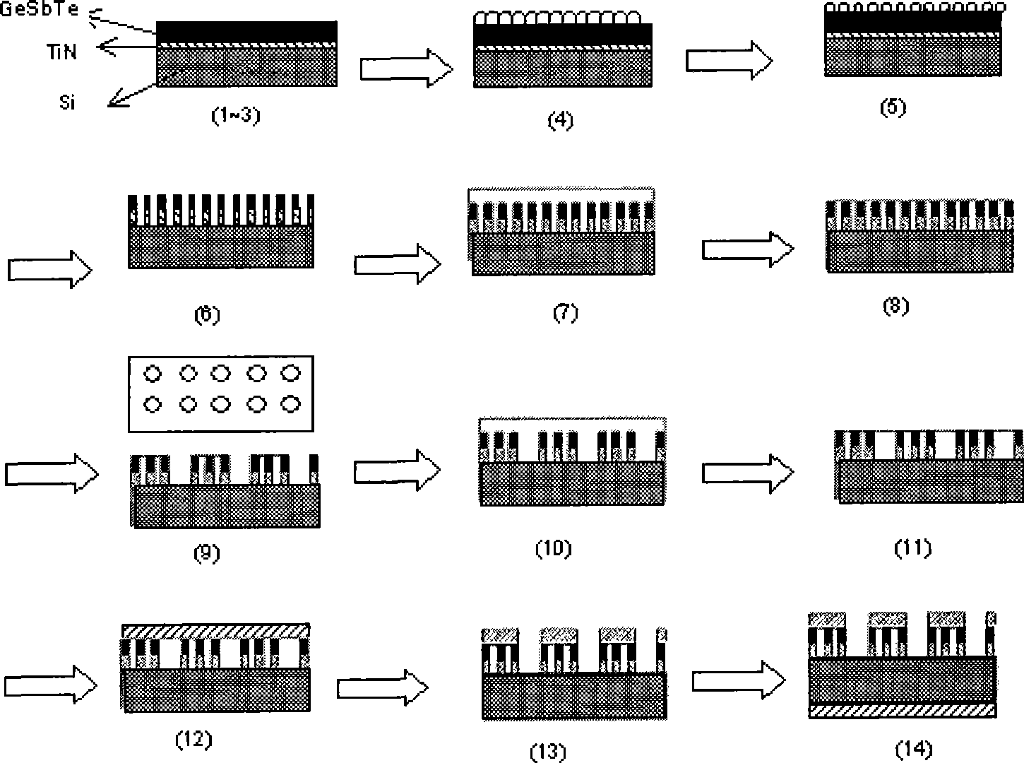
[0027] In this example, the method for preparing a sub-30 nanometer-scale chalcogenide compound nano-lattice vertical structure phase-change memory is as follows: figure 1 shown, including the following steps

[0028] 1. Prepare the substrate - select n+ or p+ type single-sided polished silicon wafer as the substrate, firstly clean it by boiling sulfuric acid + hydrogen peroxide, then rinse it with deionized water and dry it.

[0029] 2. Plating a heat-insulating layer—use a magnetron sputtering method (sputtering conditions: pressure: 0.2 Pa, substrate temperature: 550° C.) to vapor-deposit a 50-100 nanometer TiN layer as a heat-insulating layer.

[0030] 3. Coating film layer - use magnetron sputtering method (conditions: vacuum degree: 2 × 10 -4 Pa; sputtering pressure: 0.15Pa) evaporation thickness of 100-150 nanometer germanium antimony tellurium or silicon antimony tellurium thin film material.

[0031] 4. Laying templates—laying single-layer polystyrene pellets (50 to...


PUM

PropertyMeasurementUnit
diameteraaaaaaaaaa
heightaaaaaaaaaa
pore sizeaaaaaaaaaa

Abstract

The invention relates to a method for preparing a phase change memory with a vertical structure, and belongs to the technical field of nano-electronic and nano-optoelectronic devices. The method comprises the steps of substrate preparing, thermal protective layer plating, thin layer plating, template laying, ion etching, template removing, thermal insulation layer plating, polishing and planishing, photoengraving and corroding, thermal insulation layer re-plating, re-polishing and planishing, and electrode manufacturing. The method adopts nano-array phase change material as a carrier for information storage, improves the thermal efficiency of the phase change active region through introducing a proper dielectric layer between the electrode and the phase change material, ensures that the operating current and the power consumption of the memory device are effectively reduced, and has the advantages of simple process and low cost, thereby providing the foundation for the commercial memory which is suitable for PCRAM.

Description

technical field [0001] The invention relates to a method for preparing a vertical structure phase-change memory, which is a method for preparing a sub-30 nanometer-scale vertical structure with a chalcogenide compound nano-lattice as an active layer by combining photolithography and nanosphere etching technology The method for phase change memory belongs to the technical field of nanometer electronics and nanometer optoelectronic devices. Background technique [0002] Chalcogenide compound germanium antimony tellurium or silicon antimony tellurium (GexSbyTez) (SixSbyTez) phase-change semiconductor memory (referred to as PCRAM) is a new type of semiconductor memory. High performance, long cycle life, low power consumption, multi-level storage, high-speed reading, anti-interference and other advantages. However, in order to make PCRAM devices show superiority and competitiveness compared with commercial memories, they must be made into nanoelectronic devices, especially as th...

Claims


Application Information

Patent Timeline
Patent Type & Authority Applications(China)
IPC IPC(8): H01L21/822B82B3/00H01L45/00G11C11/56
Inventor 徐岭徐骏马忠元刘东廖远宝戴明杨菲刘文强吴良才陈坤基李伟
Owner NANJING UNIV
Why Eureka
Try Eureka