Method for preparing AlxGa(1-x)N triplet alloy semiconductor film at normal temperature

A ternary alloy and semiconductor technology, applied in semiconductor/solid-state device manufacturing, chemical instruments and methods, crystal growth, etc., can solve problems such as substrate or pre-buried layer thermal damage, device performance degradation, thin film function degradation, etc., to achieve High degree of ionization, lower preparation temperature, and growth-promoting effects

Inactive Publication Date: 2009-08-26
FUDAN UNIV
View PDF0 Cites 7 Cited by
  • Summary
  • Abstract
  • Description
  • Claims
  • Application Information

AI Technical Summary

Problems solved by technology

For some applications or the manufacture of certain devices, long-term high-temperature environments may cause thermal damage to the substrate or pre-buried layer, resulting in film function degradation and device performance degradation or even failure.

Method used


Image

  • Method for preparing AlxGa(1-x)N triplet alloy semiconductor film at normal temperature

Examples


Embodiment 1

[0022] Embodiment 1: Al on Si substrate 0.5 Ga 0.5 Preparation of N(x=0.5) thin films

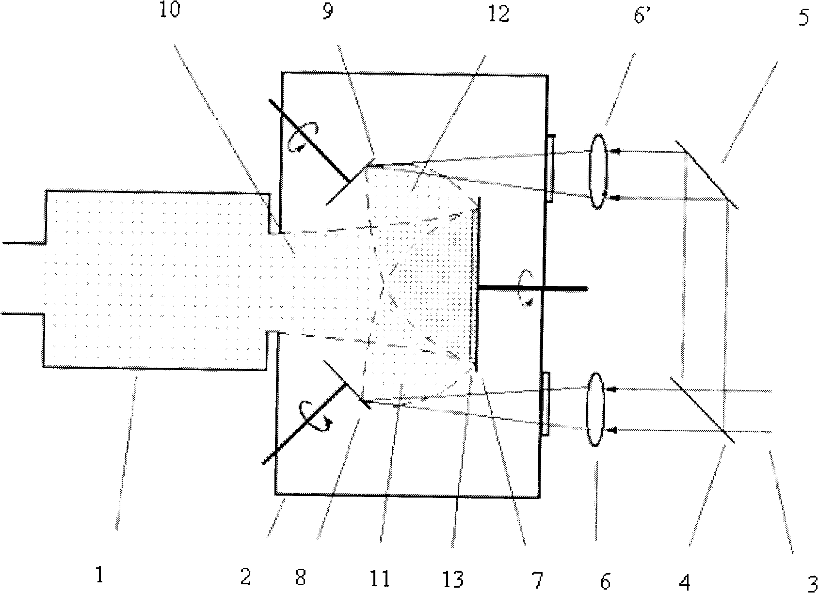
[0023] Al 0.5 Ga 0.5 The preparation device of N thin film is figure 1Configuration, 3 is Q-switched Nd:YAG laser output wavelength of 266, 355, 532 or 1064nm, repetition frequency of 1, 2, 5, 10 or 20Hz, pulse energy of 20-200mJ pulse laser beam, 8 is the purity of 99.995 % metal aluminum target, 9 is a polycrystalline AsGa target with a purity of 99.99%, 7 is a surface-polished and chemically cleaned single crystal Si (100) substrate, the aluminum target 8 and the AsGa target 9 are placed symmetrically with respect to the Si substrate 7 , the aluminum target 8, the AsGa target 9 and the Si substrate 7 are controlled by a motor outside the film forming chamber to rotate at a constant speed of tens of revolutions per minute. Vacuum the discharge chamber 1 and the film-forming chamber 2 to 10 -3 -10 -6 After Pa, fill the discharge chamber with high-purity nitrogen with a purity of 99....

Embodiment 2

[0024] Embodiment two: Al 2 o 3 Preparation of AlN(x=1) Thin Films on Substrates

[0025] AlN thin film preparation device according to figure 1 Configuration, 3 is Q-switched Nd:YAG laser output wavelength of 266, 355, 532 or 1064nm, repetition frequency of 1, 2, 5, 10 or 20Hz, pulse energy of 20-200mJ pulse laser beam, 8 is the purity of 99.995 % metallic aluminum target, no AsGa target, 7 for surface polished and cleaned single crystal Al 2 o 3 substrate, Al target 8 vs. Al 2 o 3 The position of the substrate 7 is the same as that of the aluminum target relative to the Si substrate in Example 1, and the aluminum target 8 and the Al target 2 o 3 The substrate 7 is controlled by a motor outside the film forming chamber to rotate at a constant speed of tens of revolutions per minute. Vacuum the discharge chamber 1 and the film-forming chamber 2 to 10 -3 -10 -6 After Pa, fill the discharge chamber with high-purity nitrogen with a purity of 99.999% to 10 -1 -10 -2 Pa...

Embodiment 3

[0026] Example three: SiO 2 Preparation of GaN(x=0) Thin Films on Substrates

[0027] GaN thin films were prepared by figure 1 Configuration, 3 is the Q-switched Nd:YAG laser output wavelength of 266, 355, 532 or 1064nm, repetition frequency of 1, 2, 5, 10 or 20Hz, pulse energy of 20-200mJ pulsed laser beam, 9 is the purity of 99.99 % polycrystalline AsGa target, no Al target, 7 for surface polished and cleaned SiO 2 substrate, AsGa target 9 versus SiO 2 The position of the substrate 7 is the same as that of the AsGa target relative to the Si substrate in Embodiment 1, and the AsGa target 9 and the SiO 2 The substrate 7 is controlled by a motor outside the film forming chamber to rotate at a constant speed of tens of revolutions per minute. Vacuum the discharge chamber 1 and the film-forming chamber 2 to 10 -3 -10 -6 After Pa, fill the discharge chamber with high-purity nitrogen with a purity of 99.999% to 10 -1 -10 -2 Pa is used as the working gas to keep the gas in a...


PUM

PropertyMeasurementUnit
thicknessaaaaaaaaaa

Abstract

The invention relates to a method for preparing AlxGa(1-x)N triplet alloy semiconductor film at normal temperature. The method utilizes the same laser bean to obtain two laser beans through a beam splitter mirror, wherein, one laser bean ablates aluminum target and provides aluminum for a film layer, and the other laser bean ablates AsGa target and provides gallium for the film layer; active nitrogen formed by nitrogen microwave discharge provides nitrogen for the film layer provides nitrogen for the film layer, and the aluminum, the gallium and the nitrogen which have gas phase react to form the AlxGa(1-x)N alloy semiconductor film that is sedimentated on a substrate. The invention provides a method for preparing AlxGa(1-x)N film with different aluminum-gallium ratio, especially high aluminum component at normal temperature, and the non-balancing characteristics lead the components forming the film layer to break through the restriction of equilibrium solid solubility. The two laser beans ablate the pulse laser of the two targets to trigger plasma such as laser with supersaturation, high ionizability and high expansion, etc. Plasma which has high chemical activity and formed by microwave discharge is used for assist film formation, thus greatly reducing the preparing temperature of the AlxGa(1-x)N film.

Description

technical field [0001] The present invention relates to a normal temperature preparation method of a thin film material, in particular to a process of plasma-assisted double laser beam double target co-ablation to synthesize and prepare Al with different aluminum-gallium component ratios, especially high-aluminum components, under normal temperature conditions. x Ga 1-x A method for N ternary alloy semiconductor thin films. Background technique [0002] Ternary alloy Al x Ga 1-x N is a wide-gap semiconductor material with excellent direct energy band structure, and its energy gap width Eg can be changed in the range of 3.4-6.2eV with the different aluminum content (0≤x≤1), corresponding to the light The lower limit of the response wavelength can be changed in the range of 200-365nm, and it also has a high breakdown field strength (1-3×10 10 V / cm), high electron saturation drift rate (2.2×10 10 cm / s), as well as good physical, chemical and thermal stability, have importa...

Claims


Application Information

Patent Timeline
Patent Type & Authority Applications(China)
IPC IPC(8): C30B25/00C30B29/38H01L21/205
Inventor 吴嘉达孙剑方芳干洁
Owner FUDAN UNIV
Why Eureka
Try Eureka