Compound cantilever beam needle point used for micro-nano microtechnique and manufacturing method thereof

A technology of composite cantilever beam and microscopic technology, which is applied in the field of composite cantilever beam tip and its production for micro-nano microscopic technology, and can solve problems such as complex structure, small field of view, and difficulty in realization

Inactive Publication Date: 2010-04-14
BEIJING UNIV OF TECH
View PDF0 Cites 4 Cited by
  • Summary
  • Abstract
  • Description
  • Claims
  • Application Information

AI Technical Summary

Problems solved by technology

Although the laser displacement sensor can be positioned more accurately, it is precisely because of its existence that it is difficult to realize the coupling of the scanning probe fiber system with the transmission electron microscope system or scanning electron fiber system due to the complexity of the structure. , even if realized, due to structural limitations, the coupling of the two cannot maximize the advantages of the two
[0003] In a series of articles published since 2002, the M.A.Haque research group mentioned that a nanomechanical sensor for transmission electron microscopy and scanning electron microscopy was fabricated using MEMS technology, and two mark positions were made on the sensor to ...

Method used


Image

  • Compound cantilever beam needle point used for micro-nano microtechnique and manufacturing method thereof
  • Compound cantilever beam needle point used for micro-nano microtechnique and manufacturing method thereof
  • Compound cantilever beam needle point used for micro-nano microtechnique and manufacturing method thereof

Examples


specific Embodiment

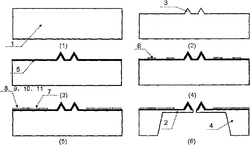
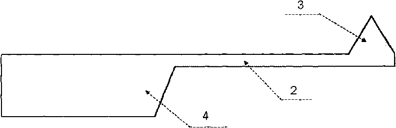
[0029] 1. Use a silicon wafer with a diameter of 2 inches, an N-type (001) surface, and a thickness of 1 mm as the substrate. The front surface uses a mask and anisotropic wet etching to produce a needle tip with a height of 7 μm, a base with a length of 3 mm, and a width of 1 mm. 500 μm, 40 μm wide cantilever.

[0030] 2. Fabricate a silicon dioxide insulating dielectric layer on the front and back of the silicon wafer with a thickness of 200nm.

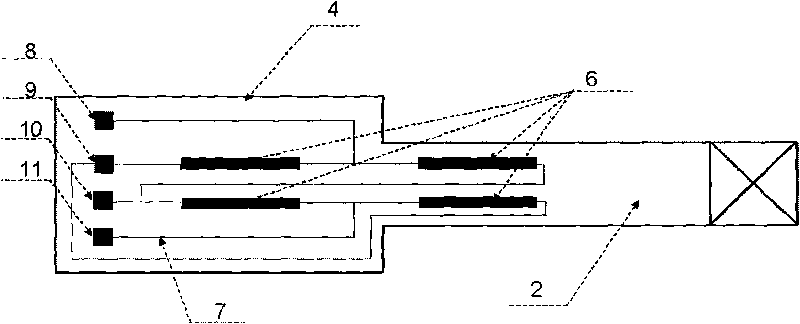
[0031] 3. The first photolithography on the silicon dioxide insulating dielectric layer using nickel-chromium alloy (Ni 80 Cr 20 ) to produce 4 piezoresistors, all of which have a resistance value of 120Ω, 2 are located on the base, and 2 are located on the cantilever beam and parallel to the length direction of the cantilever beam.

[0032] 4. On the prepared piezoresistor, use gold for the second photolithography to make a wire with a thickness of 100nm and a width of 5μm and 4 electrodes I and electrode II with a thickness of 1...


PUM


Abstract

The invention relates to a compound cantilever beam needle point used for a micro-nano microtechnique and a manufacturing method thereof. The compound cantilever beam needle point comprises a base, a cantilever beam and a needle point and is characterized in that the base, the cantilever beam and the needle point are respectively provided with an insulating dielectric layer which is distributed with four pressure-sensitive resistors with same resistance value, wherein two pressure-sensitive resistors are positioned on the base, and the other two pressure-sensitive resistors are positioned on the cantilever beam and distributed uniformly with the direction being parallel to the length direction of the cantilever beam; and the four pressure-sensitive resistors are connected into a Wheatstone bridge by wires. The compound cantilever beam needle point does not use laser positioning to measure small strain generated by the cantilever beam needle point of a scanning probe microscope, can couple the pressure-sensitive resistors capable of measuring the small strain accurately with the cantilever beam needle point so as to measure dynamical signals when the cantilever beam and a sample act, as well as information of magnitude of electrostatic force and distribution of magnetic field and the like. The invention belongs to the technical field of micro-mechanical sensors.

Description

technical field [0001] The invention relates to a composite cantilever beam tip used in micro-nano microscopy technology and a manufacturing method thereof. Using the composite cantilever beam tip of the invention will no longer use laser positioning and measurement scanning probe microscopes (atomic force microscope, electrostatic force microscope, magnetic force microscope, etc.) Microstrain, etc.) of the cantilever beam tip, but the piezoresistor that can accurately measure the tiny strain is coupled with the cantilever beam tip, and the mechanical signal and the electrostatic force when the cantilever beam interacts with the sample are measured. The information, such as the distribution of the magnetic field, belongs to the technical field of micromechanical sensors. Background technique [0002] With the development of nanotechnology, the requirements for testing methods of micro-nano signals (force, electricity, magnetism, light, etc.) are becoming stronger and stronge...

Claims


Application Information

Patent Timeline
IPC IPC(8): B81B7/02B81C1/00G12B21/02H01J37/04H01J37/28H01J37/26
Inventor 韩晓东岳永海张泽
Owner BEIJING UNIV OF TECH
Why Eureka
Try Eureka