Multichannel carbon nanotube sensor and preparation method thereof
A carbon nanotube and carbon nanotube composite technology, which is applied in the field of microelectronics, can solve the problems of unreliable contact between carbon nanotubes and electrodes, the inability to promote large-scale integrated manufacturing and use, and poor compatibility of IC integrated circuits.
- Summary
- Abstract
- Description
- Claims
- Application Information
AI Technical Summary
Problems solved by technology
Method used
Image
Examples
preparation example Construction
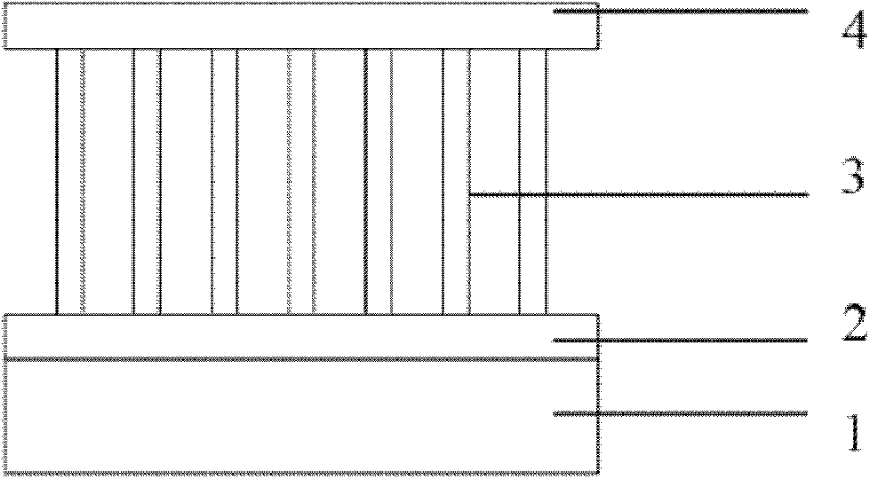
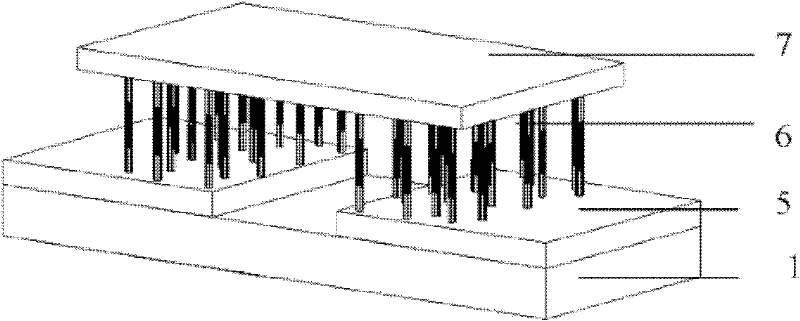
[0045] 1. Utilize the common PECVD method (plasma-enhanced chemical vapor deposition method) for preparing carbon nanotube field emission cathode arrays to obtain uniformly oriented multi-walled carbon nanotube arrays on silicon wafers deposited with nickel metal catalysts, using conventional photolithography The patterning process enables the nickel catalyst to be patterned on the silicon wafer, thereby realizing the patterning treatment of the conductive channel of the carbon nanotube, and the length of the carbon nanotube is 10 μm;
[0046] 2. Spin-coat the photoresist on the substrate to cover the carbon nanotube array. The thickness of the photoresist is 15 μm, bake the glue, and grind the photoresist with sandpaper so that the thickness of the photoresist is about 8 μm
[0047] 3. Use a sodium hydroxide solution with a concentration of 0.5% to control the etching of the photoresist for 30 seconds; 4. Deposit a Cr / Cu seed layer on the surface of the above structure, wherei...
Embodiment 2
[0056] 1. Utilize the common PECVD method (plasma-enhanced chemical vapor deposition method) for preparing carbon nanotube field emission cathode arrays to obtain uniformly oriented multi-walled carbon nanotube arrays on silicon wafers deposited with iron metal catalysts. The length is 10 μm;
[0057] 2. Spin-coat the photoresist on the substrate to cover the carbon nanotube array. The thickness of the photoresist is 15 μm, bake the glue, and grind the photoresist with sandpaper so that the thickness of the photoresist is about 8 μm
[0058] 3. Conduct photolithographic patterning on the conductive channel of carbon nanotubes, and perform RIE etching to remove the exposed carbon nanotubes after deglue, and fill them with spin-coated photoresist;
[0059] 4. Use a sodium hydroxide solution with a concentration of 0.6% to perform controlled etching on the photoresist for 25 seconds;
[0060] 5. Deposit a Cr / Cu seed layer on the surface of the above structure, wherein the Cr thi...
Embodiment 3
[0069] The carbon nanotube sensor preparation process based on the carbon nanotube finished product is as follows:
[0070] 1. Purify the multi-walled carbon nanotubes with a length of 10 μm obtained by the usual preparation method, mix them with photoresist in proportion, the mass ratio of carbon nanotubes and photoresist is 1:8, and mix them with a ball mill for 5 Hour;
[0071] 2. Spin-coat 8 μm photoresist on the silicon wafer and pattern it, then spin-coat the mixture of photoresist and carbon nanotubes, fill and cover the patterned photoresist pattern, dry, and grind with sandpaper until Expose the first layer of photoresist;
[0072] 3. Use a sodium hydroxide solution with a concentration of 0.4% to perform controlled etching on the photoresist for 40 seconds;
[0073] 4. Deposit a Cr / Cu seed layer on the surface of the above structure, wherein the thickness of Cr Cu thickness is
[0074] 5. Spin-coat photoresist on the above-mentioned Cr / Cu seed layer and patte...
PUM
| Property | Measurement | Unit |
|---|---|---|
| thickness | aaaaa | aaaaa |
| depth | aaaaa | aaaaa |
| thickness | aaaaa | aaaaa |
Abstract
Description
Claims
Application Information


