
CuxSe/TiO2 nanotube array of p-type semiconductor nano material and preparation method thereof

A nanotube array and nanomaterial technology, applied in the field of p-type semiconductor nanomaterial CuxSe/TiO2 nanotube array and its preparation, can solve the problems of only absorption, insufficient specific surface area, easy damage, etc.

Inactive Publication Date: 2010-10-27
HUNAN UNIV
View PDF9 Cites 23 Cited by
  • Summary
  • Abstract
  • Description
  • Claims
  • Application Information

AI Technical Summary

Problems solved by technology

However, the applied anodic oxidation voltage is generally only in the range of 10-25V, beyond this voltage range, the nanotube-like structure cannot be formed, which limits the diameter of the nanotube to a certain extent, and the nanotubes prepared in the aqueous solution system The tube wall is thin and easy to break
200410021589.X discloses a preparation method of titanium dioxide nanotube arrays with a high aspect ratio. The solute of the electrolyte is fluoride and supporting electrolyte, the solvent is water, and alcohol additives are added. This kind of nanotube is still relatively short, only 250 nanometers long, the specific surface area is not large enough, and it can only absorb light in the ultraviolet region, so it cannot make full use of natural sunlight.

Method used


Image

  • CuxSe/TiO2 nanotube array of p-type semiconductor nano material and preparation method thereof
  • CuxSe/TiO2 nanotube array of p-type semiconductor nano material and preparation method thereof
  • CuxSe/TiO2 nanotube array of p-type semiconductor nano material and preparation method thereof

Examples


Embodiment 1

[0023] (1) Grinding the surface of the base material, cleaning it for later use;

[0024] (2) Electrolyte preparation: the electrolyte is composed of hydrofluoric acid with HF mass percentage of 0.5-3% and dimethyl sulfoxide or NH4F with an alcohol solution of 0.25-0.5% by mass;

[0025] (3) Under 25-100V DC voltage, using pure titanium or titanium alloy as the anode and platinum sheet as the cathode, electrolytically prepare titanium oxide nanotubes in the electrolyte;

[0026] (4) Calcining the titanium oxide nanotube array prepared above under aerobic conditions at 400°C-500°C for 4-6h to crystallize it into TiO 2 nanotube arrays;

[0027] (5) adopt the Cu / TiO that step (4) obtains 2The composite nanotube array is the anode, and the platinum sheet is the cathode two-electrode system. The electrode spacing is 2cm, the voltage is 0.5V, and it is electrooxidized in 0.5M-2M NaOH alkaline solution for 30min without stirring to obtain ultrafine Cu. 2 O inner rice noodle modifi...


PUM

PropertyMeasurementUnit
diameteraaaaaaaaaa

Abstract

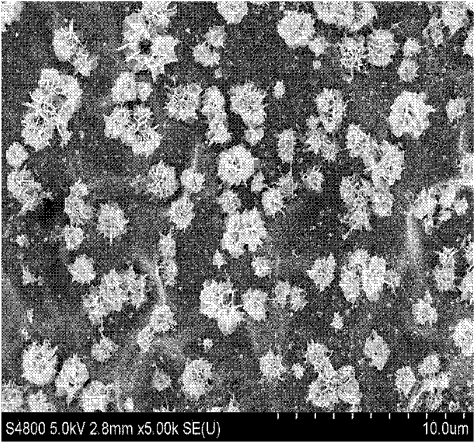
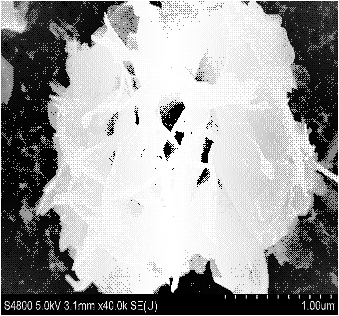
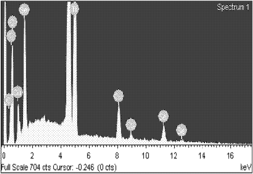
The invention discloses a CuxSe / TiO2 nanotube array of a p-type semiconductor nano material and a preparation method thereof. The method comprises the following steps: putting a TiO2 nanotube array in 5mmol-20mmol of CuSO4 solution; electrodepositing elementary substance Cu on the TiO2 nanotube array by adopting pulse plating in a standard three-electrode system to obtain a Cu / TiO2 compound nanotube array; carrying out electrooxidation in an NaOH alkaline solution for a certain time after deposition is ended to obtain a superfine Cu2O nanowire-modifying TiO2 nanotube array; and then putting the Cu2O / TiO2 nanotube array in a selenium ion solution, and stirring for 30-60 min under light to obtain a copper selenide nanotube array. Based on the superfine Cu2O nanowire-modifying TiO2 nanotube array, the absorption range of TiO2 in a visible light area can be effectively expanded and the compounding probability of an electron hole pair can be reduced, and more photoelectrons and photoholes can be generated under visible light, thereby being more beneficial to Cu2O to react with the selenium ion solution to generate copper selenide. The CuxSe / TiO2 nano material with a novel structure has potential application in the aspects of solar batteries, solar radiation absorbers, nano switches, thermoelectric photoelectric converters, superconductors, air-sensitive sensors and the like.

Description

technical field [0001] The invention belongs to the field of nanomaterial chemistry, in particular to a novel p-type semiconductor nanomaterial Cu with excellent photoelectric properties x Se / TiO 2 Nanotube arrays and methods of making them. Background technique [0002] Titanium dioxide nanotube arrays prepared by anodic oxidation have excellent characteristics such as large specific surface area and adjustable pore size. Its special nanotube-like structure has become a research hotspot in the scientific field of various countries. The electrolyte for preparing titanium dioxide nanotube arrays by anodic oxidation is usually an inorganic aqueous solution system. Since various ions migrate relatively fast in aqueous solution, the electrochemical anodic oxidation is also fast, and nanotube arrays can be formed in a relatively short time. However, the applied anodic oxidation voltage is generally only in the range of 10-25V, beyond this voltage range, the nanotube-like struct...

Claims


Application Information

Patent Timeline
Patent Type & Authority Applications(China)
IPC IPC(8): C25D11/26H01L31/18H01L31/0264
CPCY02P70/50
Inventor 罗胜联杨丽霞李玥刘承斌
Owner HUNAN UNIV
Learn More