Preparation process of amorphous silicon film solar battery based on laser etched and crystallized optical film layer

A solar cell, amorphous silicon thin film technology, applied in sustainable manufacturing/processing, circuits, electrical components, etc., can solve the problems of poor stability, low photoelectric conversion efficiency, etc., achieve low cost, easy to form large-scale production capacity, The effect of short energy recovery time

Inactive Publication Date: 2010-11-10
SHANGHAI UNIV
View PDF1 Cites 12 Cited by
  • Summary
  • Abstract
  • Description
  • Claims
  • Application Information

AI Technical Summary

Problems solved by technology

But at the same time, the disadvantages of a-Si are also obvious, ma

Method used


Image

  • Preparation process of amorphous silicon film solar battery based on laser etched and crystallized optical film layer
  • Preparation process of amorphous silicon film solar battery based on laser etched and crystallized optical film layer
  • Preparation process of amorphous silicon film solar battery based on laser etched and crystallized optical film layer

Examples


Embodiment 1

[0025] Embodiment one: the specific process steps of the present embodiment are as follows:

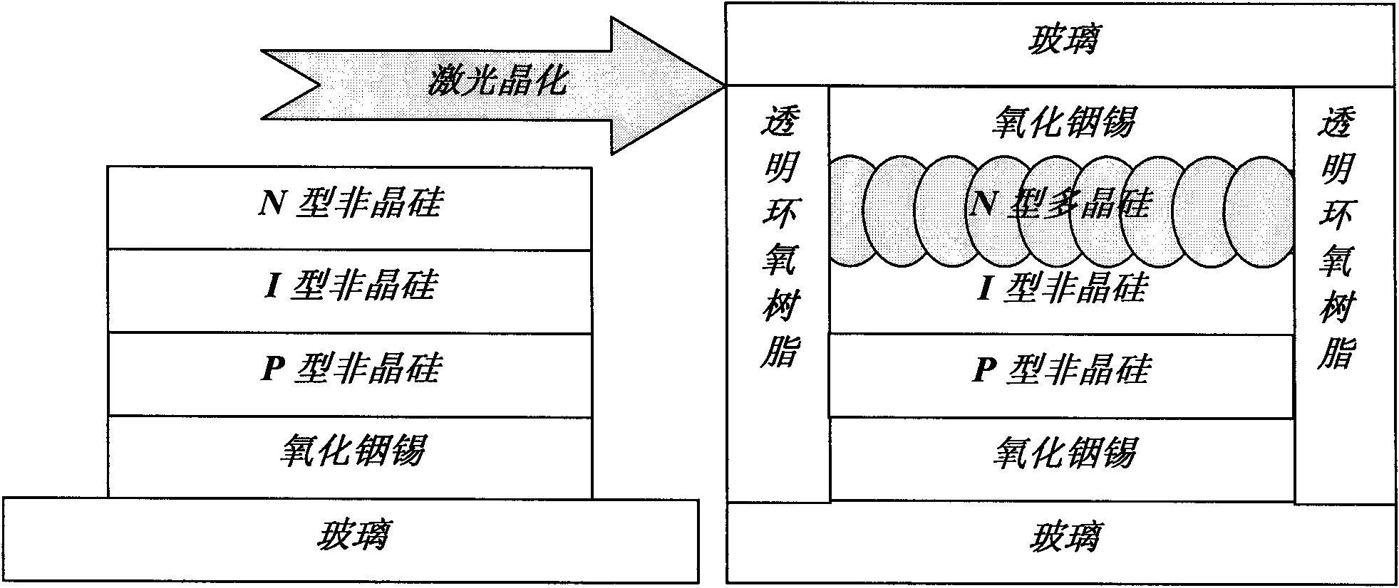
[0026] PECVD is used to prepare a-Si, the RF power is 35W, the power source capacitive coupling is 13.56MHz, the substrate temperature range is 180-250°C, and the gas glow pressure range is below 20Pa. The method includes the following process steps:

[0027] a. Preparation of P-type layer a-Si: Borane B 2 h 6 with silane SiH 4 The mass flow ratio is 0.28%, and the thickness is 30nm.

[0028] b. Type I layer (intrinsic layer) a-Si preparation: silane SiH 4 with hydrogen H 2 The mass flow ratio is 10%, and the thickness is 500 nm.

[0029] c. Preparation of N-type layer a-Si: Phosphine PH 3 with silane SiH 4 The mass flow ratio is 0.55%, and the thickness is 100nm.

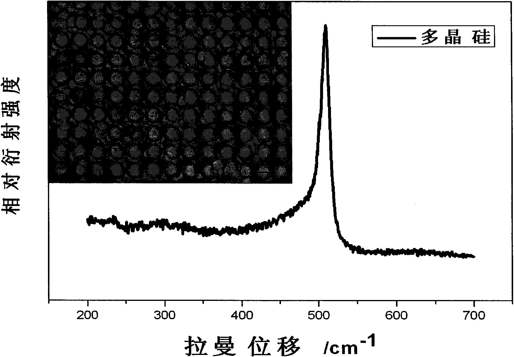
[0030] d. Preparation of the poly-Si layer of the optical thin film layer: use a frequency-doubled Nd:YAG laser with a wavelength of 532nm to irradiate the surface of the sample, and then shape it into a flat-top ...

Embodiment 2

[0033] Embodiment 2: This embodiment is basically the same as the above-mentioned embodiment, the difference is:

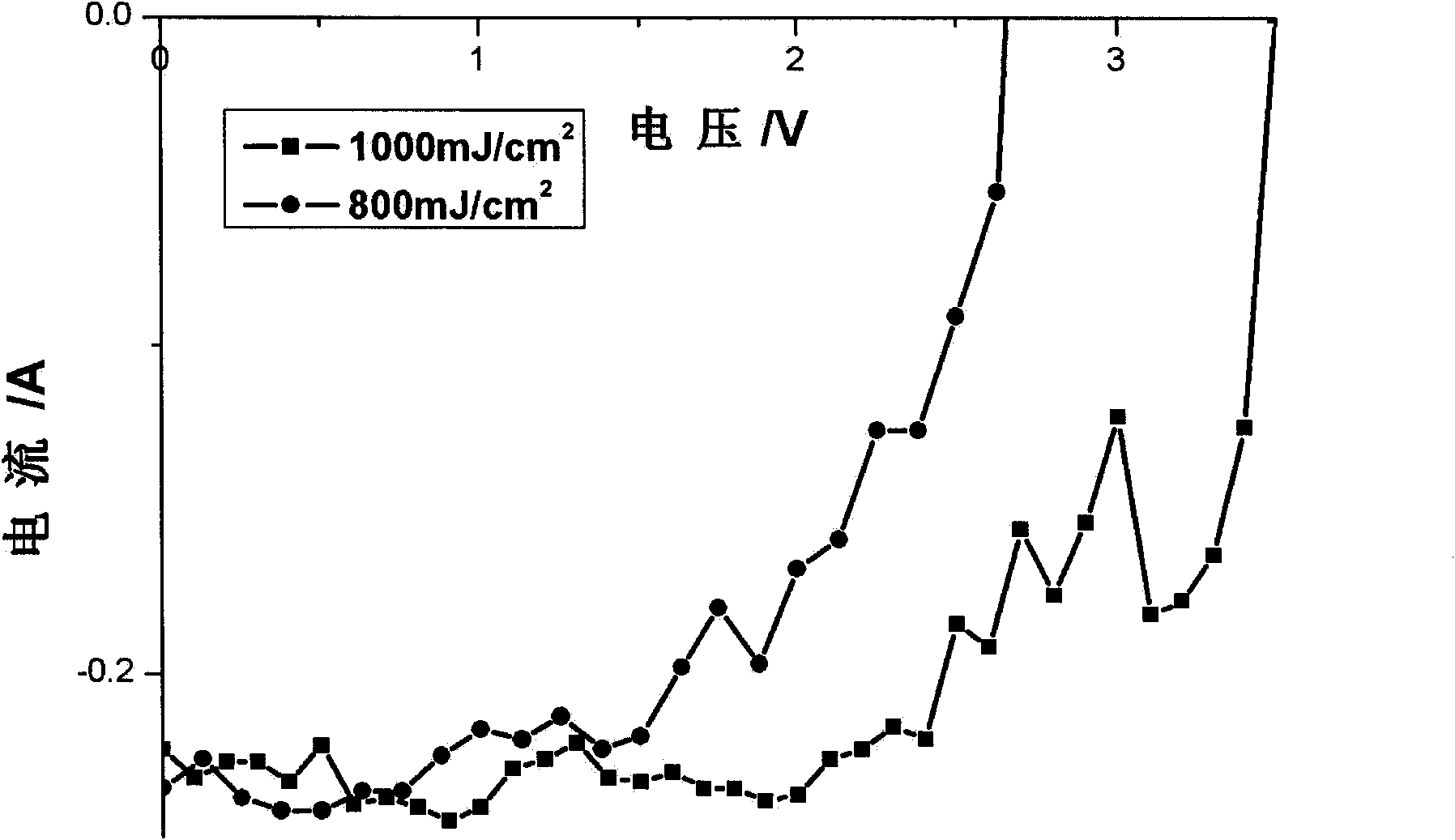
[0034] The preparation of the poly-Si layer of the optical thin film layer: the surface of the sample is irradiated with a frequency-doubled Nd:YAG laser with a wavelength of 532nm, shaped into a flat-top green laser by the fly-eye technique, and then etched and crystallized N-type amorphous silicon layer to realize N The type layer is changed from amorphous silicon to polysilicon optical thin film layer. Mainly adjust the laser energy density to control the grain size to achieve the antireflection and antireflection functions of the modulated optical film layer. Now adjust the laser energy density to 1200mJ / cm 2 .

[0035] The amorphous silicon thin-film solar cell of the polysilicon optical thin-film layer that the inventive method makes is fully suitable for the requirement of the photoelectric conversion efficiency of photoelectric solar cell, can be used as ...


PUM

PropertyMeasurementUnit
Thicknessaaaaaaaaaa
Thicknessaaaaaaaaaa
Thicknessaaaaaaaaaa

Abstract

The invention relates to a preparation process of a novel amorphous silicon film solar battery based on a laser etched and crystallized optical film layer, which belongs to the technical field of inorganic material solar device preparation. An optical film comprises an antireflective film, a transmission increasing film, a reflection increasing film and the like, and the invention achieves the reflection increasing and transmission increasing functions of a modulation optical film layer mainly by controlling the grain size. The method comprises the following steps of: depositing three layers of amorphous silicon (a-Si) films respectively in a P type, an I type and an N type on indium tin oxide (ITO) conductive glass by a plasma-enhanced chemical vapor deposition (PECVD) method, and then irradiating the surface of a sample by using frequency-doubled Nd YAG laser with the wavelength of 532nm to realize the conversion of an N type layer from amorphous silicon to a polycrystalline silicon (poly-Si) optical film layer. The polycrystalline silicon grain size of the crystallized optical film layer is controlled by changing the laser energy density to regulate the photoelectric conversion efficiency. The inorganic material solar energy of the invention can be applied to solar automobile film glass and building film glass curtain walls.

Description

technical field [0001] The invention relates to a preparation process of an amorphous silicon thin film solar cell based on laser etching crystallization of an optical thin film layer, and belongs to the technical field of inorganic material solar cells. Background technique [0002] Affected by the extreme shortage of high-purity silicon raw materials, the development of a new generation of amorphous silicon (a-Si) thin-film solar cells is very important in the solar photovoltaic industry in the world today. Due to the multiple defects of a-Si, doping often further increases the defect density. The basic structure of a-Si solar cells is not a PN junction, but a PIN junction. The heavily doped P and N regions form a built-in potential inside the battery to collect charges. Region I is the photosensitive region, which has a high absorption coefficient for photons and completely absorbs light in the sensitive spectral region. Therefore, the thickness of the a-Si battery with...

Claims


Application Information

Patent Timeline
IPC IPC(8): H01L31/20
CPCY02P70/50
Inventor 史伟民黄璐金晶聂磊王艳廖阳方翔翔
Owner SHANGHAI UNIV
Why Eureka
Try Eureka