
Graphene optical Q-switch and application

A kind of graphene optics, graphene technology, applied in lasers, laser parts, electrical components and other directions, can solve the problems of inconvenient production and application, complex production process, wavelength sensitivity, etc., achieve low cost, is conducive to industrialization, and is conducive to The effect of industrial production

Active Publication Date: 2010-12-08
SHANDONG UNIV
View PDF0 Cites 21 Cited by
  • Summary
  • Abstract
  • Description
  • Claims
  • Application Information

AI Technical Summary

Problems solved by technology

Commonly used semiconductor saturable absorbers mainly include saturable absorber mirror (SESAM) and gallium arsenide (GaAs) devices. These two devices are not only very complicated in manufacturing process, but also very sensitive to wavelength. The absorption varies greatly, or even does not absorb; when applying, it needs to be designed according to different wavelengths, which brings great inconvenience to its production and application

Method used


Image

  • Graphene optical Q-switch and application
  • Graphene optical Q-switch and application
  • Graphene optical Q-switch and application

Examples


Embodiment 1

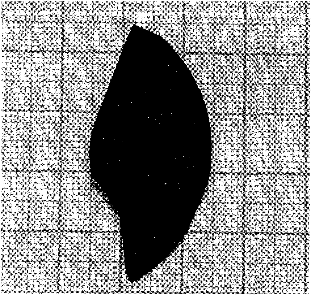
[0028] Photo of graphene grown on silicon carbide substrate as figure 1 As shown, the preparation method is to use 6H silicon carbide as the substrate and obtain it by epitaxial growth. The growth method is as described in University of Science and Technology of China, Doctoral Dissertation, Liu Zhongliang, page 102. The number of graphene layers is selected to be 10-30 layers, and the Q-switching switch can be cut into rectangles or circles according to the needs of the application. The schematic diagram of the rectangular graphene Q-switching switch is shown in figure 2 shown.

Embodiment 2

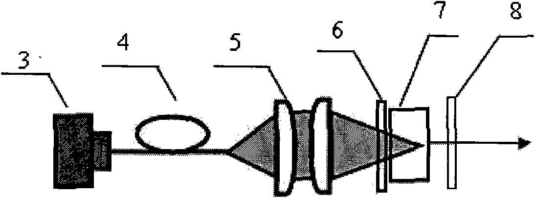
[0030] Using a laser with an emission wavelength of 808nm as the pump source and Nd:YAG crystal as the laser gain medium, adopt such as image 3 The cavity structure shown is fabricated into a pulsed laser. The laser comprises: a laser diode as a pumping source (3), a Nd:YAG crystal (6) as a laser gain medium, a coupling system (4, 5), a front cavity mirror (6) and a Q-switching element (8) of the present invention five parts. Wherein the Nd of the Nd:YAG crystal 3+ The ion concentration is 0.01-0.10 at. The pump light incident end of the Nd:YAG crystal is coated with a dielectric film that is highly transparent to 808nm and the 1.05-1.1μm band, and the output end is coated with a dielectric film that is highly transparent to the 1.05-1.1μm band. The front cavity mirror ( 6) It is a plano-concave mirror with a radius of 100-500mm, the plane is coated with 808 high-transparency, the concave surface is coated with a dielectric film with high reflection of 1.05-1.1μm, and the ...

Embodiment 3

[0032] As described in Embodiment 2, the difference is that the surface of the graphene grown on the SiC substrate of the Q-switch switch of the present invention is not coated with a dielectric film to facilitate laser oscillation.


PUM


Abstract

The invention relates to a graphene optical Q-switch and an application. The graphene optical Q-switch comprises a SiC substrate and a grapheme material growing on the SiC substrate. One surface carrying the grapheme faces the inner side of the laser cavity while the other surface faces the outer side of the laser cavity. The graphene optical Q-switch is used in the laser, pump light passes through the graphene optical Q-switch after passing through the laser gain medium and the SiC substrate is used as an output mirror and forms a resonant cavity with the front cavity mirror in front of the laser gain medium. The invention can adjust loss of laser generated by visible light, infrared or ultraviolet light. The Q-switch has the advantages of simple preparation, low cost, achievable adjustment of laser with large wavelength range and is beneficial to industrialized production and the like.

Description

technical field [0001] The invention relates to the field of laser devices, in particular to a graphene optical Q-switching device. Background technique [0002] Graphene has a two-dimensional structure of layered atomic arrangement and is a type of zero-bandgap semiconductor material. When low-power light is irradiated on graphene, electron and hole pairs will be formed on the valence band and conduction band, and then the electrons and holes will be redistributed on the conduction band and valence band respectively. After the electrons and holes are distributed It will recombine to form the distribution when it is not irradiated, which is the linear absorption process of graphene. The above process is repeated when the light is re-irradiated. However, when strong light is irradiated, all the electrons in the valence band will jump to the conduction band and form a distribution in the conduction band, so that the light will no longer be absorbed, that is, the light will m...

Claims


Application Information

Patent Timeline
IPC IPC(8): H01S3/11
Inventor 于浩海徐现刚陈秀芳张怀金胡小波王正平王继扬蒋民华
Owner SHANDONG UNIV
Learn More