

Si-base reversed extension 3C-SiC monocrystal film and preparation method thereof
A technology of single crystal thin film and deposition method, applied in the direction of single crystal growth, single crystal growth, chemical instruments and methods, etc., can solve the constraints of 3C-SiC single crystal thin film growth, large lattice mismatch coefficient, large thermal expansion coefficient, etc. problems, to achieve the effect of avoiding difficulties, high electron Hall mobility, and simple equipment
- Summary
- Abstract
- Description
- Claims
- Application Information
AI Technical Summary
Problems solved by technology
Method used
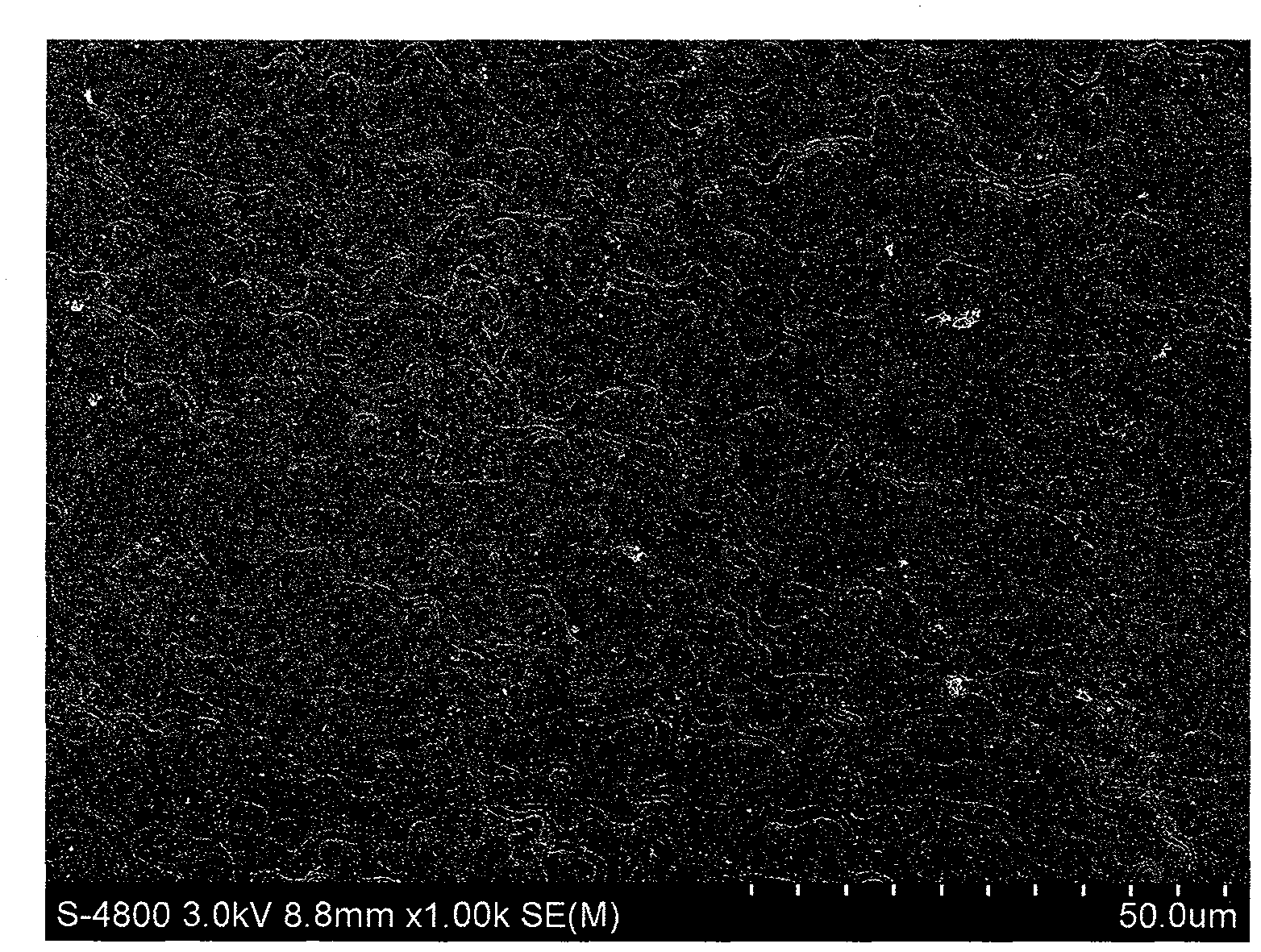
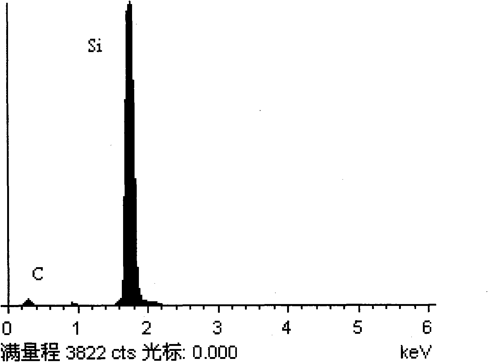
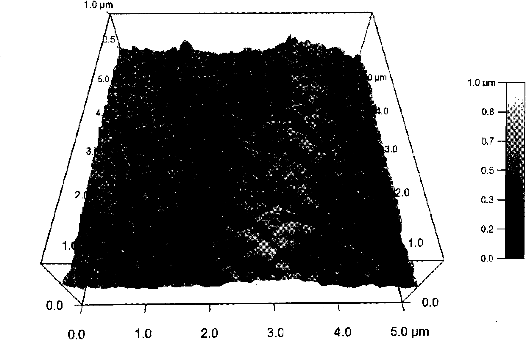
Image

Examples
Embodiment 1
[0039] Use 10 15 cm -3 3C-SiC Single Crystal Thin Films Prepared on n-Si(111) Substrates
[0040] (1) Cleaning and drying of silicon substrate
[0041] First, the silicon wafers are ultrasonically cleaned in toluene, acetone and alcohol solutions in order to remove the organic matter on the surface. Boil in a mixed solution of ammonia water and a mixed solution of deionized water, hydrogen peroxide and hydrochloric acid to remove acidic oxides and basic oxides on the surface of silicon wafers, then use a mixed solution of hydrofluoric acid and deionized water to clean the surface oxides, and finally use a large amount of The silicon wafer was rinsed with deionized water and dried, which was used as a substrate for the growth of 3C-SiC single crystal thin film.
[0042] (2) Process conditions for reverse epitaxial growth
[0043] 3C-SiC single crystal thin film is grown by LPCVD method, hydrogen gas flow is 50-200 sccm, methane gas flow is not more than 5 sccm, pressure is ...
Embodiment 2
[0048] Use 10 15 cm -3 After boron diffusion on the n-Si(111) substrate, 8×10 19 cm -3 The p-Si(111) substrate is used to prepare 3C-SiC single crystal thin film
[0049] Preparation of 3C-SiC single crystal thin films by changing the conductivity type and impurity concentration of the substrate
[0050] (1) Cleaning and drying of silicon substrate
[0051] First, the silicon wafers are ultrasonically cleaned in toluene, acetone and alcohol solutions in order to remove the organic matter on the surface. Boil in a mixed solution of ammonia water and a mixed solution of deionized water, hydrogen peroxide and hydrochloric acid to remove acidic oxides and basic oxides on the surface of silicon wafers, then use a mixed solution of hydrofluoric acid and deionized water to clean the surface oxides, and finally use a large amount of The silicon wafer was rinsed with deionized water and dried, which was used as a substrate for the growth of 3C-SiC single crystal thin film.
[005...
Embodiment 3
[0060] Use 10 15 cm -3 3C-SiC Single Crystal Thin Films Prepared on n-Si(111) Substrates
[0061] (1) Cleaning and drying of silicon substrate
[0062] Firstly, the silicon wafer is ultrasonically cleaned in toluene, acetone and alcohol solution to remove the organic matter on the surface, then the silicon wafer is heated in concentrated sulfuric acid to remove the metal impurities on the surface, and then the silicon wafer is sequentially washed in deionized water, hydrogen peroxide, ammonia water, Boil in a mixed solution of ionized water, hydrogen peroxide, and hydrochloric acid to remove acidic and basic oxides on the surface of silicon wafers, then use a mixed solution of hydrofluoric acid and deionized water to remove surface oxides, and rinse with a large amount of deionized water The silicon wafer is dried and used as the substrate for growing 3C-SiC single crystal thin film.
[0063] (2) Process conditions for reverse epitaxial growth
[0064] LPCVD method to grow...
PUM
| Property | Measurement | Unit |
|---|---|---|
| Thickness | aaaaa | aaaaa |
| Hall mobility | aaaaa | aaaaa |
Abstract
Description
Claims
Application Information