Method for manufacturing three-dimensional smooth curved surface microstructure based on SU-8 thick photo-resist

A production method, SU-8 technology, applied in the direction of microstructure technology, microstructure device, manufacturing microstructure device, etc., can solve the problems of high glass transition temperature, difficult to use positive photoresist reflow method, etc. simple effect

Active Publication Date: 2011-01-19
SHANGHAI INST OF MICROSYSTEM & INFORMATION TECH CHINESE ACAD OF SCI
View PDF6 Cites 23 Cited by
  • Summary
  • Abstract
  • Description
  • Claims
  • Application Information

AI Technical Summary

Problems solved by technology

However, due to the high glass transition temperature of the cross-linked SU-8 material, which is close to its carbonization and pyrolysis temperature, it is di

Method used


Image

  • Method for manufacturing three-dimensional smooth curved surface microstructure based on SU-8 thick photo-resist
  • Method for manufacturing three-dimensional smooth curved surface microstructure based on SU-8 thick photo-resist
  • Method for manufacturing three-dimensional smooth curved surface microstructure based on SU-8 thick photo-resist

Examples


Embodiment 1

[0016] The substantive features and remarkable progress of the present invention will be further described below in conjunction with the accompanying drawings using SU-8 photoresist.

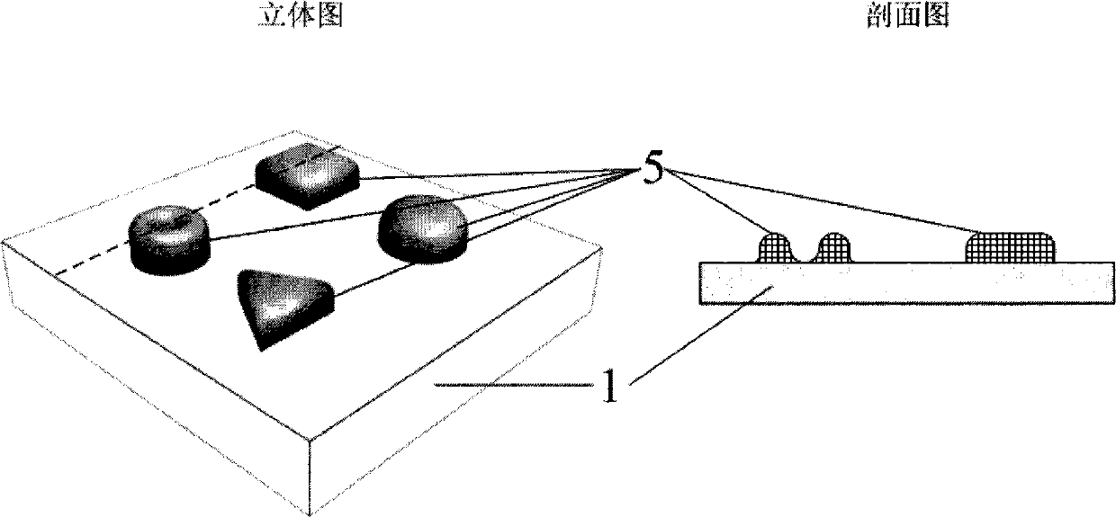
[0017] 1. Utilize SU-8 photoresist conventional process to make SU-8 original model, such as figure 1 shown.

[0018] 2. Mix the PDMS prepolymer and curing agent in a ratio of 10:1 (mass ratio), and vacuum degas (eliminate the bubbles formed by stirring and mixing the PDMS prepolymer and curing agent), and pour it into the SU- 8 on the original mold, and then placed on a hot plate at 85°C for 1 hour to cure.

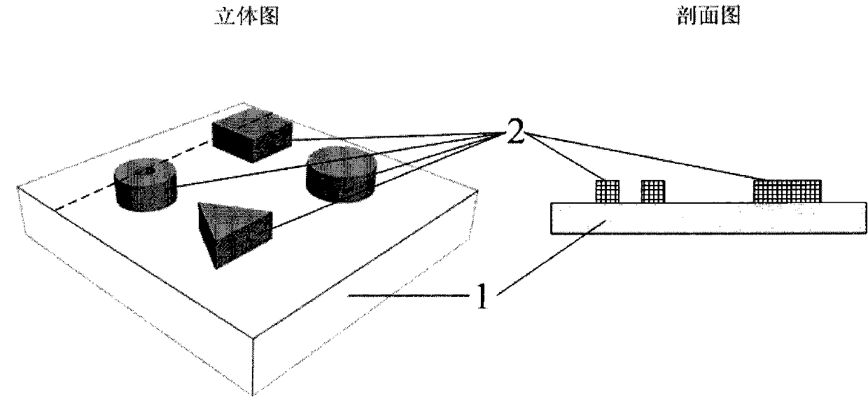
[0019] 3. Peel off the cured PDMS from the SU-8 master mold to make a PDMS master mold, such as figure 2 shown.

[0020] 4. Take the cleaned silicon wafer, bake at 150°C for 20 minutes, cool to room temperature, spin-coat SU-8 photoresist, place on a hot plate at 90°C and bake for 1 hour, then cool to room temperature.

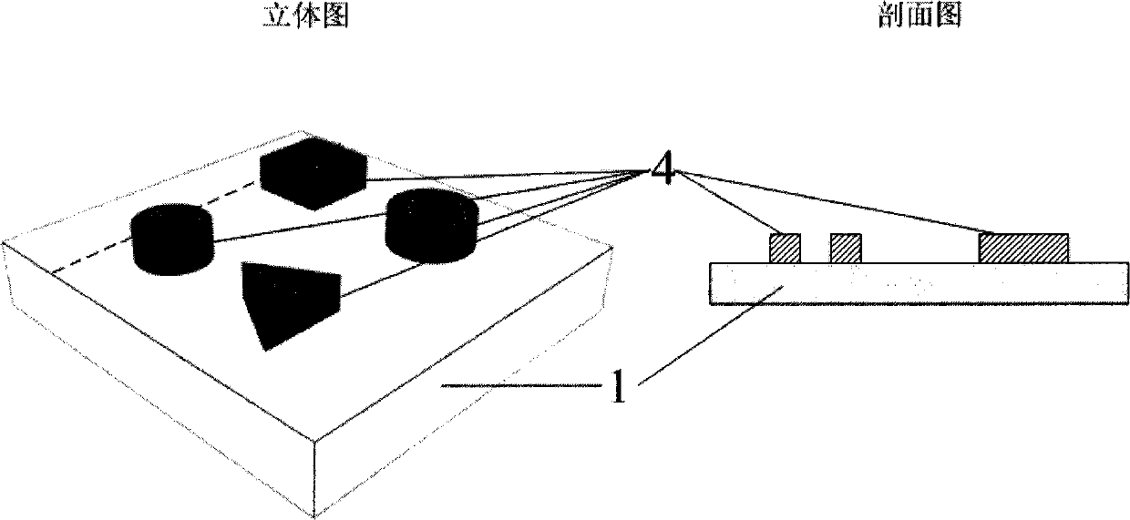
[0021] 5. After vacuum degassing the PDMS master mold prepared a...

Embodiment 2

[0024] Utilize the process method of making the SU-8 smooth surface microstructure that embodiment 1 proposes to make microlens arrays with different curvatures (such as Figure 5 shown), the curvature of the microlens can be controlled by adjusting the thickness of the SU-8 master mold and the size and shape design of the light-transmitting structure of the photolithography mask. The thickness of the SU-8 master mold is between 10 μm and 1000 μm, and the photolithography mask The shape of the light-transmitting structure of the stencil can be a regular polygon or a circle, and the side length or diameter is 10 μm-1000 μm. The fabricated microlens array can be applied to fields such as flat panel display, three-dimensional stereoscopic imaging, fiber optic coupler, micro-focusing, and micro-projection.


PUM

PropertyMeasurementUnit
Thicknessaaaaaaaaaa

Abstract

The invention discloses a method for manufacturing a three-dimensional smooth curved surface microstructure based on SU-8 thick photo-resist. The method is characterized in that the microstructure with smooth curved surface characteristic is manufactured by combining stamping technology of polydimethyl siloxane (PDMS) and the refluxing characteristic of non-crosslinked SU-8 photo-resist. The method comprises the following steps of: manufacturing an SU-8 master die by photo-etching technology; pouring PDMS to form a female die by using the master die; converting the PDMS female die into an SU-8 male die by using the stamping technology; stripping the PDMS die; and refluxing the SU-8 male die which is not subjected to exposure and cross-linking reaction under the environment of high temperature of between 55 and 120 DEG C to form the three-dimensional microstructure with smooth curved surface characteristic. Compared with the conventional gray scale mask technology, diverging light exposure technology and positive photo-resist refluxing method, the smooth curved surface microstructure provided by the invention has the characteristics of simple and convenient machining, low cost, stable structure, large structure curvature range and the like.

Description

technical field [0001] The present invention relates to a kind of fabrication method of smooth curved surface microstructure, relate to the fabrication method of three-dimensional smooth curved surface microstructure based on SU-8 thick photoresist more precisely, described method can be applied to MEMS (Micro Electromechanical System, namely microelectromechanical systems) field. Background technique [0002] SU-8 glue is a negative, epoxy resin type, UV-sensitive thick photoresist, suitable for making microstructures with high aspect ratio, due to its excellent mechanical, optical properties, chemical resistance and thermal stability In recent years, SU-8 has been widely used in the field of MEMS, including MOEMS (micro-opto-electromechanical systems), microfluidics, machinery, sensors, actuators, biochips, micro-gears, and calibration tools. important structural material. At present, the conventional SU-8 manufacturing process is made by traditional microelectronic proc...

Claims


Application Information

Patent Timeline
IPC IPC(8): G03F7/00B81C1/00
Inventor 李刚陈强沈念赵建龙
Owner SHANGHAI INST OF MICROSYSTEM & INFORMATION TECH CHINESE ACAD OF SCI
Why Eureka
Try Eureka