Seed crystal for growth of silicon carbide single crystal, process for producing the same, and silicone carbide single crystal and process for producing the same

A technology of silicon carbide single crystal and manufacturing method, which is applied in the directions of single crystal growth, single crystal growth, crystal growth, etc., can solve problems such as reduced effect and reduced gas barrier property, and achieves suppression of crystal defects, excellent gas barrier property, and gas barrier properties. High barrier effect

Active Publication Date: 2011-05-11
RESONAC CORPORATION
View PDF3 Cites 27 Cited by
  • Summary
  • Abstract
  • Description
  • Claims
  • Application Information

AI Technical Summary

Problems solved by technology

The cracked gas makes the protective film porous and lowers the gas barrier properties.
Therefore, the effect of suppressing the sublimation of the seed crystal is reduced

Method used


Image

  • Seed crystal for growth of silicon carbide single crystal, process for producing the same, and silicone carbide single crystal and process for producing the same
  • Seed crystal for growth of silicon carbide single crystal, process for producing the same, and silicone carbide single crystal and process for producing the same
  • Seed crystal for growth of silicon carbide single crystal, process for producing the same, and silicone carbide single crystal and process for producing the same

Examples


Embodiment approach 1

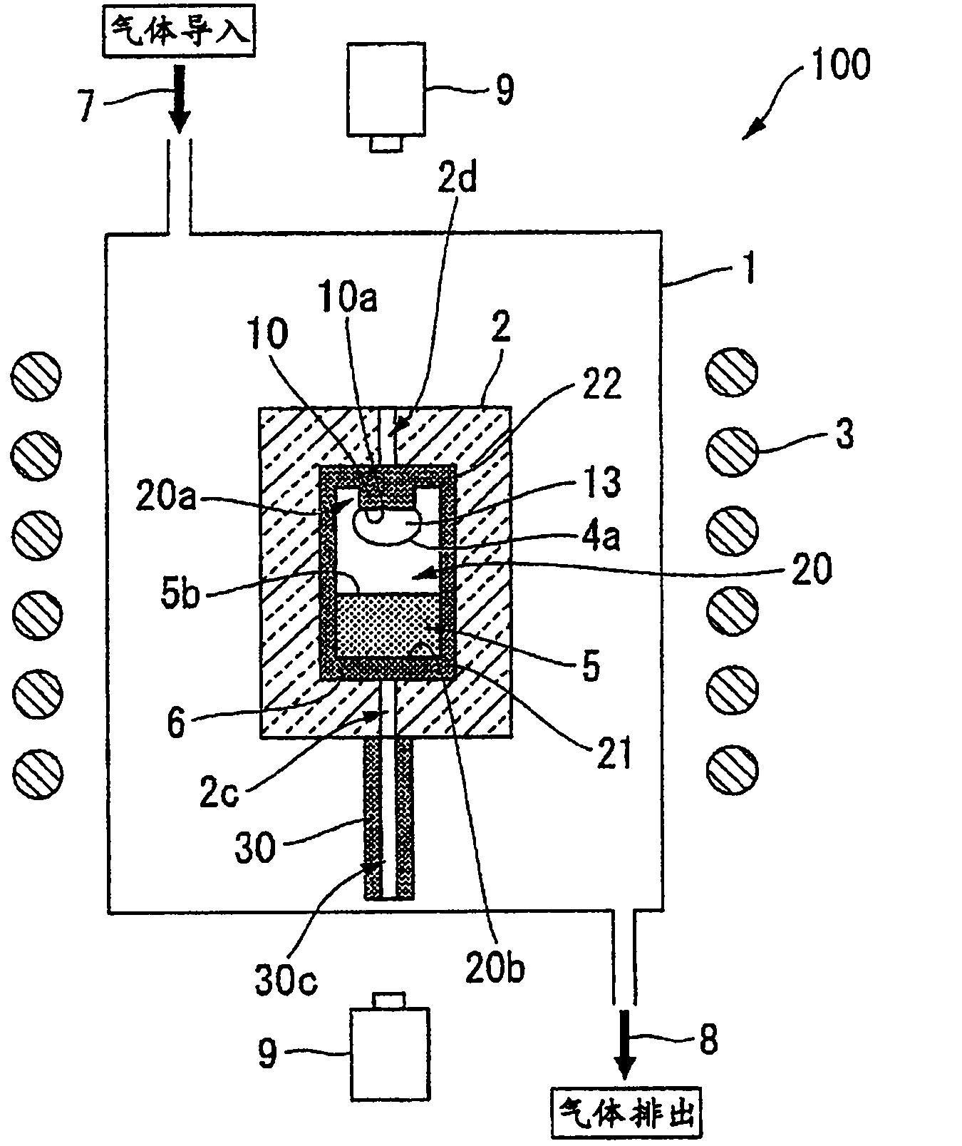
[0045] figure 1 It is a figure for demonstrating an example of the seed crystal for silicon carbide single crystal growth which is embodiment of this invention. It is a schematic cross-sectional view showing an example of a crystal growth apparatus in which a seed crystal for growing a silicon carbide single crystal according to an embodiment of the present invention is arranged.

[0046] Such as figure 1 As shown, the crystal growth apparatus 100 is schematically configured by arranging a graphite crucible 6 covered with a heat insulating (heat insulating) material 2 inside a vacuum container 1. A seed crystal 13 for growing a silicon carbide single crystal according to an embodiment of the present invention is bonded to one surface 10a of the protruding portion 10 of the cover 22 .

[0047] As the material of the vacuum vessel 1, a material capable of maintaining a high vacuum is preferably used, for example, quartz, stainless steel, and the like.

[0048] In addition, as...

Embodiment 1

[0123] First, prepare a substrate with an area of ​​about 1.5cm 2 , a silicon carbide seed crystal substrate composed of 4H-silicon carbide single crystal with a thickness of 0.3mm, which was washed with a sulfuric acid-hydrogen peroxide mixed solution at 10°C for 10 minutes, washed with ultrapure water for 5 minutes, and ammonia- Wash with hydrogen peroxide mixed solution for 10 minutes, wash with running water for 5 minutes with washing ultrapure water, wash with hydrochloric acid-hydrogen peroxide mixed solution for 10 minutes, wash with running water for 5 minutes with washing ultrapure water, and then wash with HF solution. Then, after oxidizing the surface at 1200°C, HF cleaning was performed again.

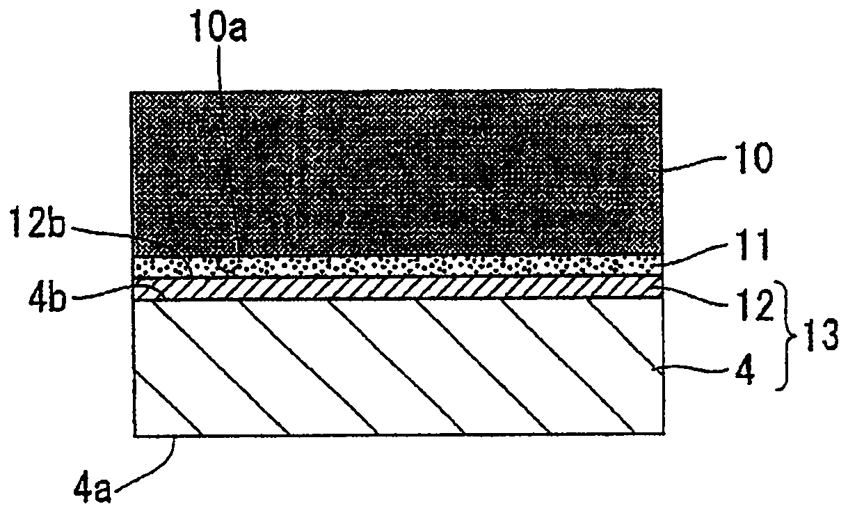
[0124] Next, a carbon film was formed on the (000-1) surface of the seed crystal substrate to form a silicon carbide single crystal growth seed crystal. As a film-forming method of the carbon film, a DC discharge sputtering method was used. The film was formed by sputteri...

Embodiment 2

[0141] In addition to using: the (000-1) plane of a 4H-silicon carbide single crystal with a thickness of 0.8 mm is used as the growth plane, and the (0001) plane is used as the surface on the side in contact with graphite, and a carbon film is formed on the (0001) plane. A silicon carbide single crystal was formed in the same manner as in Example 1 except for a growth seed crystal composed of a silicon carbide single crystal.

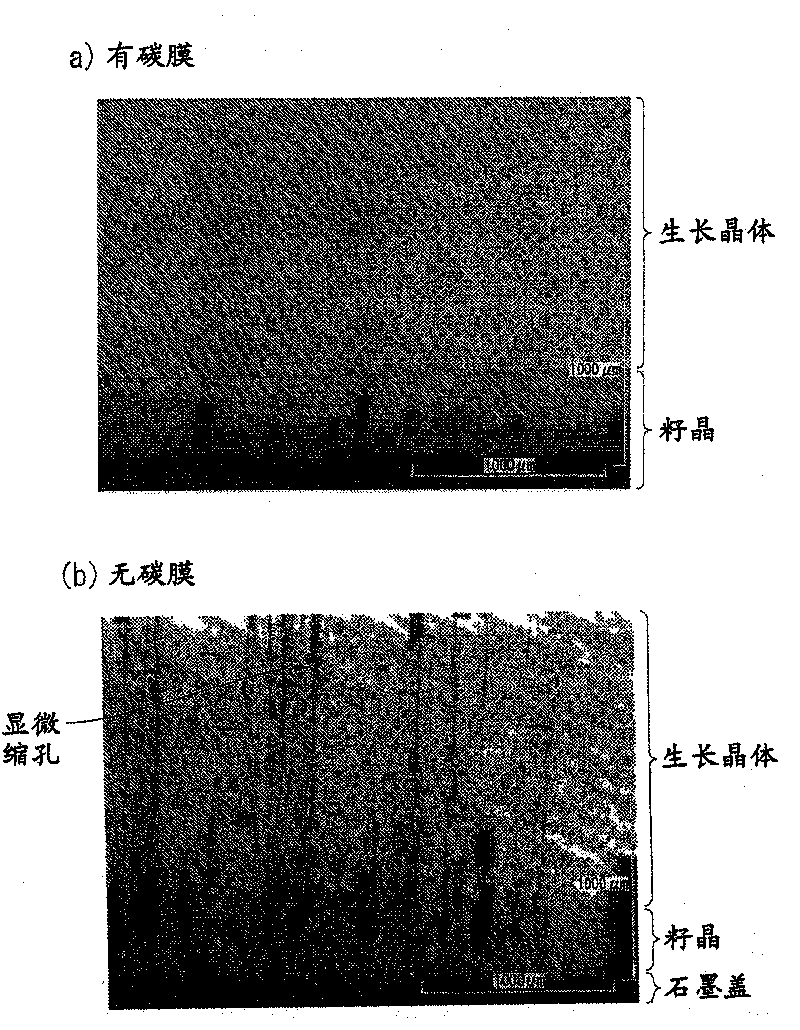
[0142] The obtained silicon carbide single crystal was cut parallel to the growth direction, and the cut surface was observed with a microscope. As in Example 1, substantially no void-like defects occurred in the silicon carbide single crystal.

[0143] From this, it was confirmed that even when the polarities of the two surfaces of the seed crystal made of silicon carbide are different, the effect of suppressing defects can be exhibited.


PUM

PropertyMeasurementUnit
densityaaaaaaaaaa
thicknessaaaaaaaaaa
thicknessaaaaaaaaaa

Abstract

A seed crystal for the growth of a silicon carbide single crystal is provided which inhibits crystal defects from generating at the interface between the seed crystal and graphite and with which a high-quality silicon carbide single crystal having a low crystal defect density can be produced with satisfactory reproducibility. The seed crystal for the growth of a silicon carbide single crystal is a seed crystal (13) for silicon carbide single-crystal growth which is to be attached to the lid of a graphite crucible filled with a raw silicon carbide powder. The seed crystal (13) comprises: a seed crystal (4) which is constituted of silicon carbide and one side of which is a growth surface (4a) where a silicon carbide single crystal is to be grown by the sublimation method; and a carbon film (12) formed on the side (4b) opposite to the growth surface of the seed crystal (4), the carbon film (12) having a density of 1.2-3.3 g / cm3.

Description

technical field [0001] The present invention relates to a seed crystal for growing a silicon carbide single crystal and a manufacturing method thereof, and a silicon carbide single crystal and a manufacturing method thereof. [0002] This application claims priority based on Patent Application No. 2008-176255 for which it applied in Japan on July 4, 2008, and uses the content of the said application in this application. Background technique [0003] Silicon carbide is a material with high thermal conductivity. In addition, they are generally physically and chemically stable, excellent in heat resistance and mechanical strength, and high in radiation resistance. Therefore, silicon carbide is used as a material for rectification elements and switching elements with high withstand voltage and low loss. In addition, silicon carbide has a wide energy band gap (forbidden band width), and in particular, a 4H-type silicon carbide single crystal has a forbidden band gap of about 3 ...

Claims


Application Information

Patent Timeline
Patent Type & Authority Applications(China)
IPC IPC(8): C30B29/36
CPCC30B23/00C30B23/025C30B29/36Y10T428/265Y10T428/263Y10T428/24273
Inventor 小柳直树小古井久雄
Owner RESONAC CORPORATION
Why Eureka
Try Eureka