Novel crystalline silicon solar cell and manufacturing method thereof

A technology of solar cells and manufacturing methods, applied in circuits, photovoltaic power generation, electrical components, etc., can solve problems such as reducing surface recombination rate, limiting battery open circuit voltage, and reducing density

Inactive Publication Date: 2011-05-18
JA SOLAR TECH YANGZHOU
View PDF5 Cites 28 Cited by
  • Summary
  • Abstract
  • Description
  • Claims
  • Application Information

AI Technical Summary

Problems solved by technology

[0005] However, for a monocrystalline silicon solar cell in which metal is directly deposited on the back of the substrate, the surface recombination on the back of the cell will reduce the density of minority carriers near the back surface, which limits the increase in the open circuit voltage of the cell.
Inserting a heavily doped back field between the absorber layer and the metal layer creates a potential barrier for photogenerated carriers, preventing the diffusion of photogenerated electrons, which helps to reduce the surface recombination rate to a certain extent, but for the entire surface For silicon wafers with metal contact areas, this method has limited effect

Method used


Image

  • Novel crystalline silicon solar cell and manufacturing method thereof
  • Novel crystalline silicon solar cell and manufacturing method thereof
  • Novel crystalline silicon solar cell and manufacturing method thereof

Examples


Embodiment 1

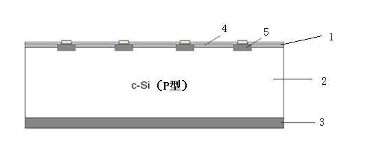
[0027] This invention is a design plan for the transformation efficiency of crystal silicon solar batteries to obtain the largest solar cell conversion efficiency.The matrix of the solar cell can use a light mixed single crystal silicon wafer with a resistance of 0.1 ~ 10 ω ?? CM is a polysilicon silicon wafer.The front surface of the substrate has a selective transmitting pole structure. This structure is a heavy diffusion under the metal grille line, and the area between the grid lines is lightly spread to obtain a low contact resistance.During the diffusion, the light diffusion zone and the heavy diffusion area have formed a conductivity that is opposite to the substrate (for example, the matrix is P type, the corresponding heavy diffusion zone and the light diffusion zone are N -type, and vice versa).A layer of reducing membrane (such as: silicon nitride or silicon dioxide, or silicon oxide and silica nitride stacks) are deposited on the front surface, and only the heavy diffu...

Embodiment 2

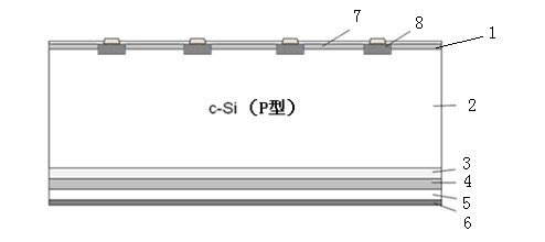
[0030] Figure 4 The solar battery structure diagram of the implementation method.A photovoltaic battery that can convert solar energy into electrical energy provided by this embodiment. The structure is as follows: a kind of conductive crystal silicon matrix, the matrix can be single crystal silicon wafers or polycrystalline silicon wafers.The front surface of the matrix has a transmitting polar structure. This structure is expanded under the metal grille line, and the regional expansion between the grid lines is lightly expanded.The first layer of reduction of the anticipation and a set of metal conductive electrode; there is a heterogeneous structure on the back of the substrate. This structure includes: the first layer covers the album of hydrococcinimum silicon (A-SI: H) membrane covering the entire back of the substrate.; The first layer adopts a doped agent with the same type of conductivity type for heavy doping of hydrogenated amorphous silicon (A-SI: H) membrane; the fir...


PUM

PropertyMeasurementUnit
thicknessaaaaaaaaaa
thicknessaaaaaaaaaa
widthaaaaaaaaaa

Abstract

The invention discloses a novel crystalline silicon solar cell. The novel crystalline silicon solar cell comprises a crystalline silicon matrix, wherein the front surface of the crystalline silicon matrix has an emitter structure, and the back surface of the crystalline silicon matrix has a heterojunction structure; the heterojunction structure comprises an intrinsically hydrogenated amorphous silicon film, a hydrogenated amorphous silicon film, a transparent conductive oxide film and a metal conductive electrode in turn; the intrinsically hydrogenated amorphous silicon film covers the entire back surface of the crystalline silicon matrix; the hydrogenated amorphous silicon film is heavily doped by using a dopant which has the same conduction type as that of the matrix; and the metal conductive electrode passes through the transparent conductive oxide film and is in ohmic contact with a heavily doped layer. The invention also discloses a manufacturing method of the crystalline silicon solar cell. The crystalline silicon solar cell with the structure can reduce composite loss on the surface; meanwhile, the back surface of the solar cell forms a better light trap structure to improve open-circuit voltage of the solar cell, so that conversion efficiency of the solar cell is improved.

Description

Technical field [0001] The invention is a photovoltaic technology field, which involves a new type of solar cell with high conversion efficiency and its production process. Background technique [0002] Photovoltaic technology is a technology that uses a large area of P-N diode to convert solar energy into electrical energy. This P-N diode is called solar cell.The semiconductor materials for making solar batteries have certain bandwidths. When solar cells are radiated by solar batteries, photons that exceed the bandwidth of the bandwidth generate electronic cave pairs in the solar cell.The asymmetric determines the flow direction of different types of photochemicals, and the power can be output to the outside through the external circuit connection.This is similar to ordinary electrochemical battery principles. figure 1 Gives the basic structure of a P-crystal silicon solar cell. [0003] The highest theoretical conversion efficiency of solar batteries formed by a single P-N junc...

Claims


Application Information

Patent Timeline
Patent Type & Authority Applications(China)
IPC IPC(8): H01L31/042H01L31/0352H01L31/0224H01L31/18
CPCY02E10/52Y02E10/50Y02P70/50
Inventor 李玉庆蒋方丹单伟
Owner JA SOLAR TECH YANGZHOU
Why Eureka
Try Eureka