Full silicon quantum dot nano laser and manufacturing method thereof

A nano-laser and silicon quantum dot technology, which is applied in the field of nano-photonic materials and new lasers, can solve the problems of difficult industrialization, high manufacturing cost, and low luminous efficiency of silicon materials, and achieve good stability and repeatability, and a wide processing range , good coherence effect

Inactive Publication Date: 2011-05-18
GUIZHOU UNIV
View PDF4 Cites 6 Cited by
  • Summary
  • Abstract
  • Description
  • Claims
  • Application Information

AI Technical Summary

Problems solved by technology

The second is the need to improve the optical properties of silicon materials. We know that the indirect bandgap structure of single crystal silicon leads to low luminous efficiency of silicon materials, and the way to improve the optical properties of silicon materials is mainly to use energy band engineering to prepare low-dimensional silicon materials. Nanostructures to obtain quasi-direct bandgap structures, such as nano-silicon, porous silicon, germanium-silicon strained layers, and nano-silicon oxide ma

Method used


Image

  • Full silicon quantum dot nano laser and manufacturing method thereof
  • Full silicon quantum dot nano laser and manufacturing method thereof
  • Full silicon quantum dot nano laser and manufacturing method thereof

Examples


Embodiment 1

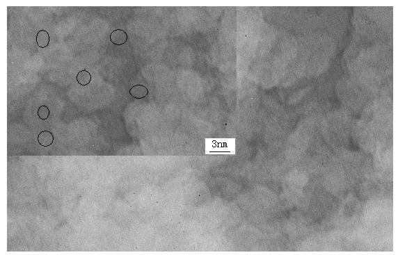
[0029] Embodiment 1: Prepare a stable all-silicon quantum dot nanolaser on the silicon surface with a nanosecond pulsed laser beam of 1064nm wavelength:

[0030] (1) Pretreatment: P-type doping is performed on the single crystal silicon wafer to form a silicon wafer with a resistivity of 2-20 ohm cm. The silicon oxide layer formed on the silicon surface in the air is removed with hydrofluoric acid, and alcohol and desiccant are used to remove the silicon oxide layer. Ionized water cleans the surface;

[0031] (2) Obtaining pulsed laser beams: use LD-pumped Nd:YAG solid-state lasers to obtain nanosecond pulsed lasers using acousto-optic Q-switching; use KTP crystals to achieve angle-matched frequency doubling, and adjust the fundamental mode output under the laser beam spot with a wavelength of 532nm ;Put the converging lens in a suitable position to converge the laser beam spot to the required line diameter; adjust the laser repetition rate to 3200 times / second, pulse width 30...

Embodiment 2

[0035] Embodiment 2: Application of all-silicon quantum dot nanolaser

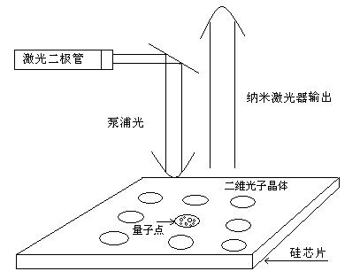
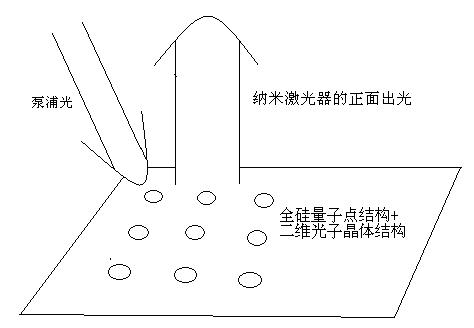
[0036] There are two options for assembling the all-silicon quantum dot nanolaser on the chip: one is to fix the optical path angle of the two-dimensional photonic crystal used as the resonance mode selection of the laser, select the optical path angle of the pump light and the outgoing light, and fix the mode output. The second is to change the optical path angle of the two-dimensional photonic crystal used as the resonance mode selection of the laser, by changing the optical path angle of the pump light and the outgoing light (such as Image 6 Shown), realize the pattern matching of wavelength division multiplexing.

[0037] As an optical interconnection application on a silicon chip, under the pumping of a short-wavelength laser, a strong stimulated light with good coherence in the visible region can be obtained (such as Figure 7 shown), which can be used for laser sources and propagation elements for...


PUM


Abstract

The invention discloses a full silicon quantum dot nano laser and a manufacturing method thereof. The nano laser is excited by optical pumping, uses full silicon quantum dots as working substance, adopts two-dimensional photonic crystals for resonant mode selection and generates laser, uses nanosecond pulse laser beams for processing and has about 100[mum] of the line diameter size of the main body, so the nano laser is the laser having the smallest volume at present; the light exit power of the laser can be up to 1 milliwatt, the light exit wavelength can be adjusted in the range from 570nm to 760nm, and the manufactured full silicon quantum dot nano laser is good in structural stability and repeatability, has outstanding light gain in the aspect of light emitting property under shortwave laser pumping, and also has excellent coherence. The manufacturing cost is low and large-scale industrial production can be easily realized.

Description

technical field [0001] The invention relates to the technical fields of nano-photonic materials and novel lasers, in particular to an all-silicon quantum dot nano-laser and a preparation method thereof. Background technique [0002] Today's development has entered into on-chip optoelectronic integration and chip-level all-opticalization, which is the key to realizing optical quantum information processing and optical quantum information calculation, and making light sources and propagation nodes for optical interconnection on silicon chips is a bottleneck. work. At present, there is an urgent need for chip-level micro-lasers and coherent light sources. [0003] Today, the microelectronic information industry based on silicon is highly developed, but due to the limitation of size and power consumption, Moore's Law has reached the limit of its applicable scope. Scientists are trying to establish a new optical quantum information processing system on silicon based on optical ...

Claims


Application Information

Patent Timeline
IPC IPC(8): H01S5/30H01S5/04
Inventor 黄伟其
Owner GUIZHOU UNIV
Why Eureka
Try Eureka