

Method for producing high-voltage grid drive chip for directly driving power device
A technology for power devices and driving chips, applied in the fields of semiconductor/solid-state device manufacturing, semiconductor devices, electrical components, etc., can solve the problems of complex process, unsatisfactory design, large leakage current, etc., to increase impurity energy and reduce lateral The effect of spreading, reducing the total thickness
- Summary
- Abstract
- Description
- Claims
- Application Information
AI Technical Summary
Problems solved by technology
Method used
Image

Examples
Embodiment 1
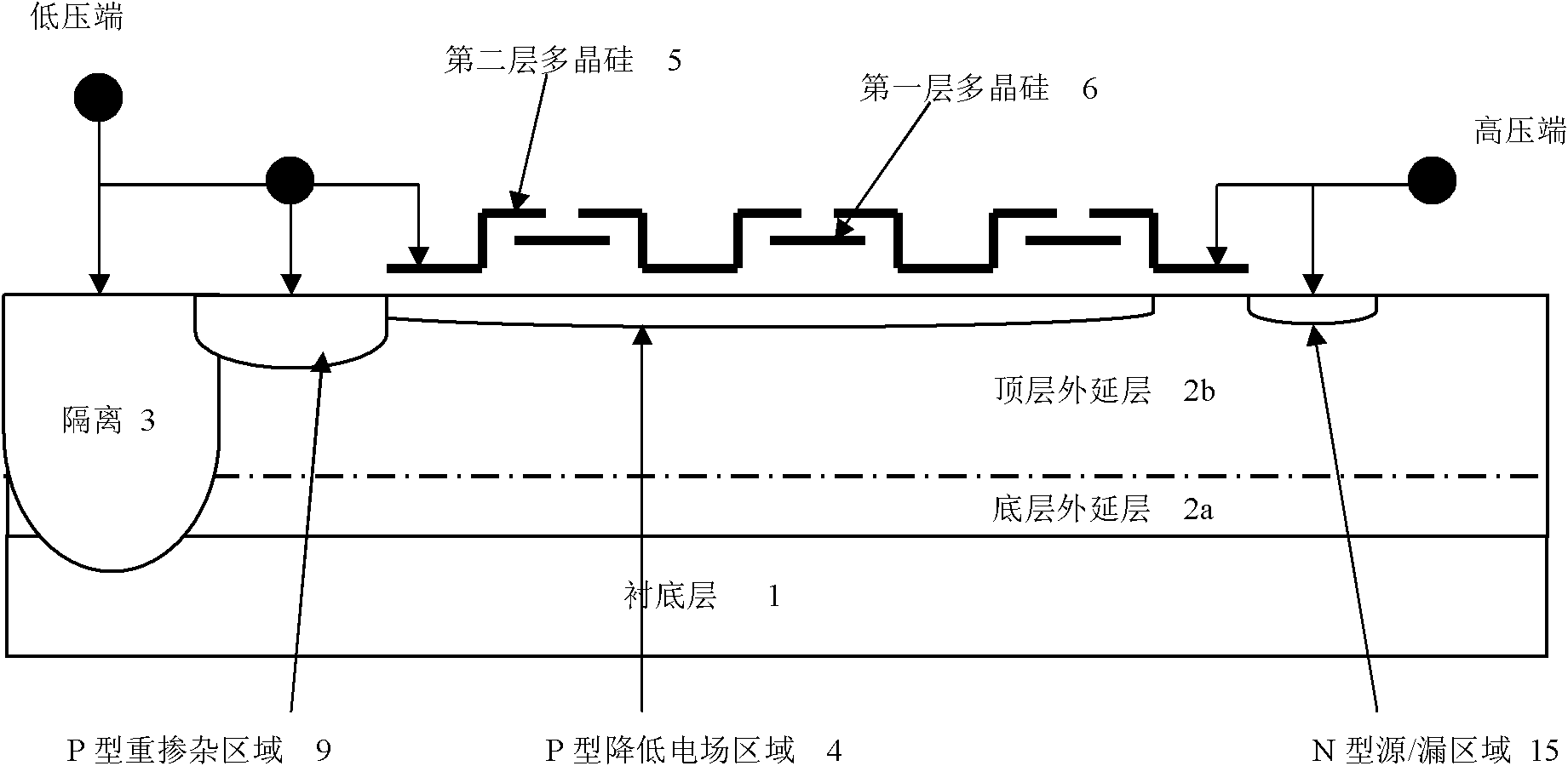
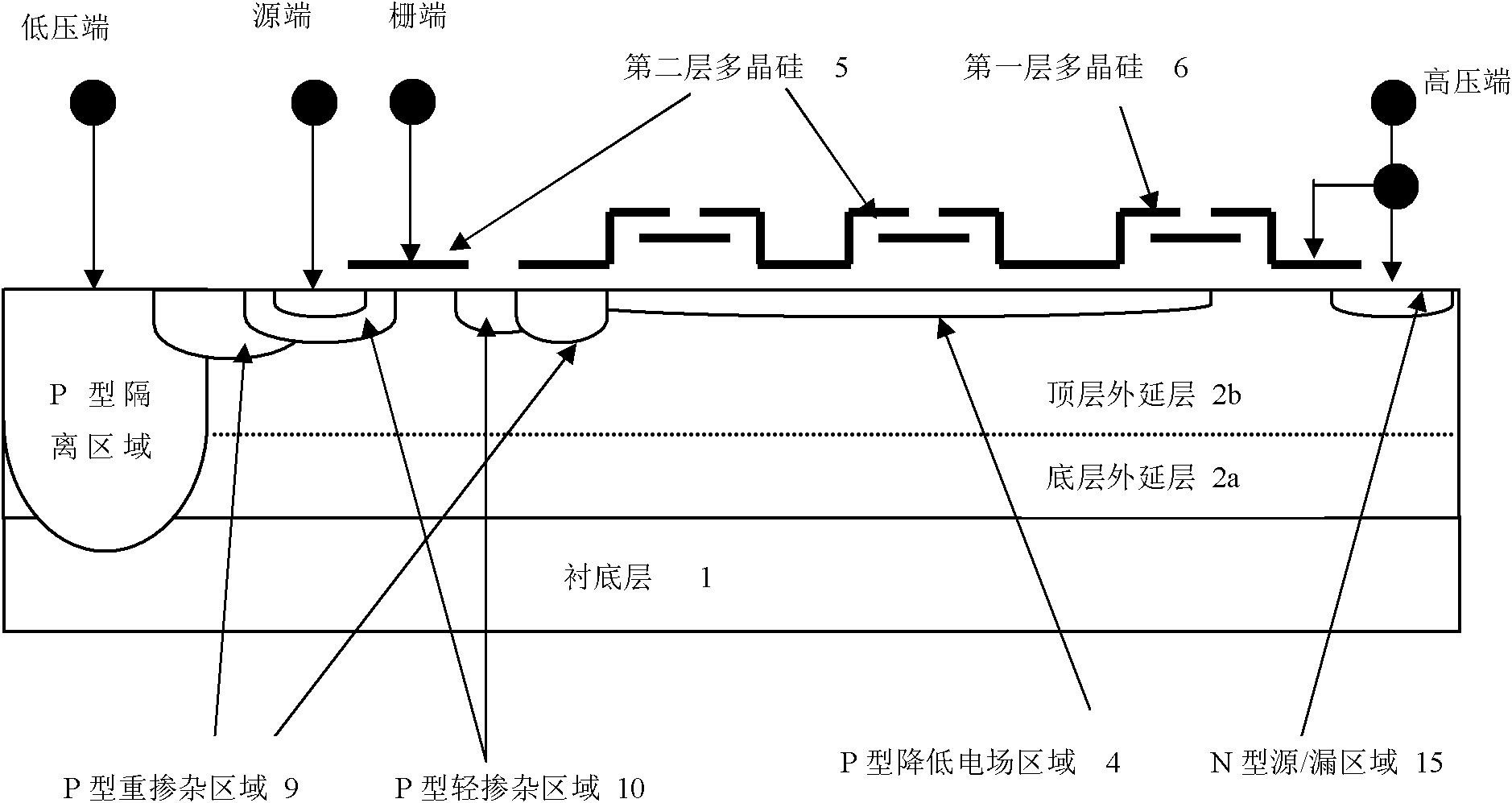
[0043] The present invention proposes a method for preparing a high-voltage gate drive chip for directly driving power devices, which is compatible with the high-voltage process and the conventional CMOS process, and on the basis of using conventional PN junction isolation, by implanting doping Boron ions form a P-type RESURF region on the N-type epitaxial layer, and at the same time use two layers of polysilicon (ie, the first layer of polysilicon and the second layer of polysilicon) on the surface of the PN junction to form a series of capacitive voltage dividers, such as figure 1 As shown, when the circuit is connected, the lower plate of the outermost capacitive voltage divider is grounded, and the upper plate of the innermost capacitive voltage divider is connected to a high potential, which effectively changes the surface electric field of the PN junction and changes the PN junction The direction of the electric force lines on the surface helps to reduce the electric fiel...
Embodiment 2
[0069] This embodiment is basically the same as Embodiment 1, and the preparation process of this embodiment is specifically as follows:
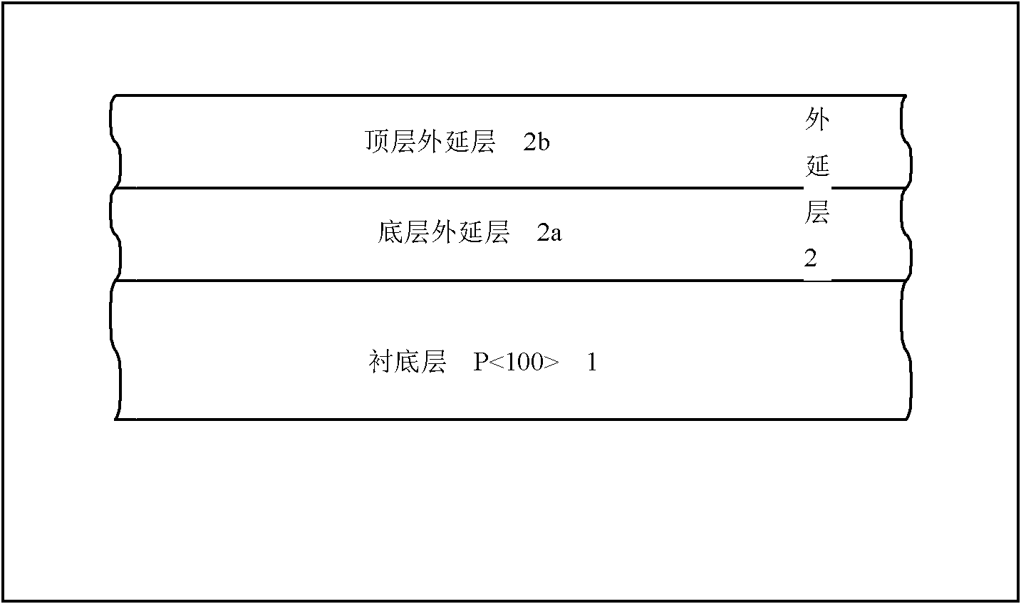
[0070] ① Material selection: select a P-type silicon wafer with a crystal orientation of (100) and a resistivity of 60ohm cm. as the initial material, and select a phosphorus-doped N-type silicon wafer as the epitaxial material. An N-type epitaxial layer 2 with a double-layer structure made of epitaxial materials is directly grown on the substrate layer, such as image 3 As shown, the epitaxial layer 2 includes a bottom epitaxial layer 2a and a top epitaxial layer 2b, and the substrate layer 1, the bottom epitaxial layer 2a and the top epitaxial layer 2b are grown sequentially from bottom to top.
[0071] ②The P-type isolation area is prepared by high-voltage junction isolation process (HVJI), such as Figure 4 As shown, the specific process is as follows:
[0072] ②-1, grow a layer of silicon dioxide with a thickness of 1100nm on the top...
Embodiment 3
[0086] This embodiment is basically the same as embodiment one and embodiment two, and the preparation process of this embodiment is specifically as follows:
[0087] ①Material selection: select a P-type silicon wafer with a crystal orientation of (100) and a resistivity of 50ohm·cm. An N-type epitaxial layer 2 with a double-layer structure made of epitaxial materials is directly grown on the substrate layer, such as image 3 As shown, the epitaxial layer 2 includes a bottom epitaxial layer 2a and a top epitaxial layer 2b, and the substrate layer 1, the bottom epitaxial layer 2a and the top epitaxial layer 2b are grown sequentially from bottom to top.
[0088] ②The P-type isolation area is prepared by high-voltage junction isolation process (HVJI), such as Figure 4 As shown, the specific process is as follows:
[0089] ②-1, grow a layer of silicon dioxide with a thickness of 1000nm on the top epitaxial layer 2b, and coat a layer of photolithographic mask layer on the silico...
PUM
 Abstract
Description
Claims
Application Information