Hydrophilic, multifunctional and integrated miniflow control chip easy to optical detection, manufacture method thereof and use thereof

A microfluidic chip, optical detection technology, applied in chemical instruments and methods, material analysis by optical means, measurement devices, etc. , to simplify the production process, facilitate fluorescence detection, and achieve the effect of good reproducibility

Inactive Publication Date: 2011-08-31
NANJING UNIV
View PDF5 Cites 21 Cited by
  • Summary
  • Abstract
  • Description
  • Claims
  • Application Information

AI Technical Summary

Problems solved by technology

However, wet etching has the following problems: 1. The control of the pattern is poor, and it cannot be used for small feature sizes (micron); 2. It will generate a large amount of chemical waste liquid
But the PDMS material is too hydrophobic, and thermoplastic chips require expensive equipment

Method used


Image

  • Hydrophilic, multifunctional and integrated miniflow control chip easy to optical detection, manufacture method thereof and use thereof
  • Hydrophilic, multifunctional and integrated miniflow control chip easy to optical detection, manufacture method thereof and use thereof
  • Hydrophilic, multifunctional and integrated miniflow control chip easy to optical detection, manufacture method thereof and use thereof

Examples


Embodiment 1

[0041] Preparation of quartz / bisphenol A epoxy acrylate-methyl methacrylate / PDMS microfluidic chip:

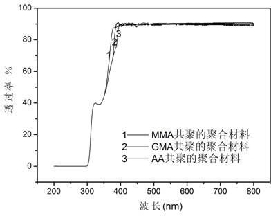
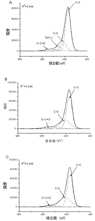
[0042] Dissolve 1 gram of bisphenol A epoxy acrylate (EBECRYL600, purchased from Cytec) in 1 gram of methyl methacrylate, add 0.05 gram of UV initiator (Irgacure184, purchased from Ciba), vortex, and sonicate for 30 minutes. Spin-coat the prepolymer evenly on the quartz substrate with a thickness of 50 microns, pre-bake at 60°C for 10 minutes, attach a mask plate containing the desired designed microstructure pattern, UV cure for 10 seconds, remove the mask plate, Bake at 80°C for 30 minutes and develop in propylene glycol acetate for 1 minute. A suitable PDMS cover slip was prepared, and after plasma treatment for 30 seconds, it was sealed with the substrate to obtain the designed microfluidic chip.

Embodiment 2

[0044] Preparation of quartz / bisphenol A epoxy acrylate-methyl methacrylate / PDMS microfluidic chip:

[0045] Dissolve 1 gram of bisphenol A epoxy acrylate (EBECRYL600 purchased from Cytec) in 1 gram of methyl methacrylate, add 0.005 gram of UV initiator (Irgacure184, purchased from Ciba Company), vortex, and sonicate for 30 minutes. Spin-coat the prepolymer evenly on the quartz substrate with a thickness of 250 microns, pre-bake at 60°C for 10 minutes, attach a mask plate containing the desired designed microstructure pattern, UV cure for 50 seconds, remove the mask plate, Bake at 80°C for 30 minutes and develop in propylene glycol acetate for 1 minute. A suitable PDMS cover slip was prepared, and after 30 seconds of plasma treatment, it was sealed with the substrate to obtain the designed microfluidic chip.

Embodiment 3

[0047] Preparation of quartz / bisphenol A epoxy acrylate-methyl methacrylate / PDMS microfluidic chip:

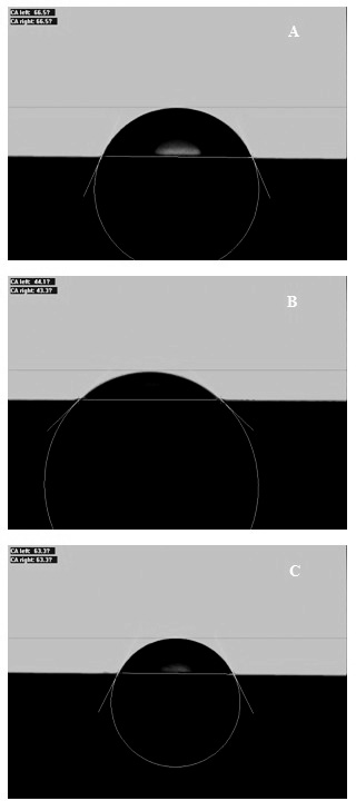
[0048] Dissolve 0.5 g of bisphenol A epoxy acrylate (EBECRYL600, purchased from Cytec) in 0.5 g of methyl methacrylate, add 0.01 g of UV initiator (Irgacure184, purchased from Ciba), vortex, and sonicate for 30 minutes. Spin-coat the prepolymer evenly on the quartz substrate with a thickness of 500 microns, pre-bake at 60°C for 10 minutes, attach a mask plate containing the desired designed microstructure pattern, UV cure for 10 seconds, remove the mask plate, Bake at 80°C for 30 minutes and develop in propylene glycol acetate for 1 minute. Prepare a suitable PDMS cover sheet, and after plasma treatment for 30 seconds, seal it with the substrate to obtain the designed microfluidic chip. See the photo of the chip Image 6 .


PUM

PropertyMeasurementUnit
thicknessaaaaaaaaaa
thicknessaaaaaaaaaa
thicknessaaaaaaaaaa

Abstract

The invention provides a hydrophilic, multifunctional and integrated miniflow control chip which is easy to optical detection, and can be manufactured on a large scale. The manufacture method of the miniflow control chip comprises the steps of coating a layer of mixtures which are as thick as 50-500 micrometers and comprise a monomer of acrylic chemical compounds containing different active groups, a cross-linking agent and an UV (ultraviolet) initiating agent on a transparent substrate, solidifying by means of ultraviolet irradiation under the cover of a required microstructural pattern-containing mask plate, removing the un-solidified cross-linking agent, initiating agent and monomer in a developing way, and sealing a cover plate to obtain the hydrophilic, multifunctional and integrated miniflow control chip easy to optical detection-adaptive. The miniflow control chip is small in nonspecific absorption, is good in biological compatibility, and can be applied to the reaction, the separation, the detection and the like of biological molecules. The miniflow control chip is easy to perform the optical detection, and is particularly suitable for the ultraviolet light absorption detection; and an intermediate higher molecular layer plays a part in optical slit without additional optical slits. Due to the active groups, the miniflow control chip is easy to integrate multifunctional operation units. The invention discloses the manufacture method of the miniflow control chip.

Description

technical field [0001] The invention relates to a preparation method of a microfluidic chip capable of hydrophilicity, multifunctional integration and easy optical detection, a main material and its application in the biological field. Background technique [0002] A microfluidic chip is a miniaturized device that integrates sample preparation, reaction, separation, detection and other operating units in the process of biological, chemical, and medical analysis into a postage stamp or credit card-sized chip, and completes a series of functions. It has the advantages of small size, multiple functions, high throughput, and less consumption of samples and reagents. It is known as one of the seven technologies that "change the world". [0003] At present, there are mainly three different systems of microfluidic chips at home and abroad: 1. Glass microfluidic chips; 2. Polydimethylsiloxane (PDMS) microfluidic chips; 3. Thermoplastic microfluidic chips. Different microfluidic chi...

Claims


Application Information

Patent Timeline
Patent Type & Authority Applications(China)
IPC IPC(8): B01L3/00G01N35/00G01N21/01
Inventor 刘震李澧
Owner NANJING UNIV
Why Eureka
Try Eureka