Manufacturing method of unimolecular sequencing chip

A single-molecule sequencing and chip technology, applied in biochemical equipment and methods, determination/inspection of microorganisms, bioreactors/fermenters for specific purposes, etc. , complex processing technology, etc.

Active Publication Date: 2015-12-02
GENEMIND BIOSCIENCES CO LTD
View PDF5 Cites 13 Cited by
  • Summary
  • Abstract
  • Description
  • Claims
  • Application Information

AI Technical Summary

Problems solved by technology

However, the second-generation sequencing chip is currently the mainstream product on the market. Most of them use semiconductor nano-processing technology to obtain high-density nano-arrays. clean room to complete
In addition, in order to achieve the purpose of high-throughput sequencing, the second-generation sequencing chip usually has a large channel width. When the negative pressure pumping method is used to inject samples for biochemical reactions, there are usually problems of uneven flow field distribution of the fluid and cover glass. The problem of easy deformation of the film
Uneven distribution of the flow field will cause unclean reagent switching and affect biochemical reactions. The deformation of the cover glass will affect the quality of the chip and even affect the collection of base optical signals.

Method used


Image

  • Manufacturing method of unimolecular sequencing chip
  • Manufacturing method of unimolecular sequencing chip
  • Manufacturing method of unimolecular sequencing chip

Examples


Embodiment 1

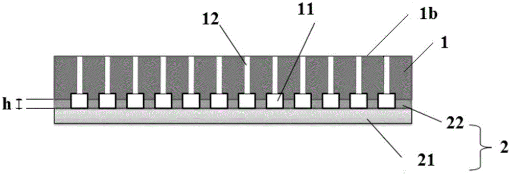
[0074] A kind of preparation method of single-molecule sequencing chip (see attached image 3 The schematic diagram of the preparation method), comprises the following steps:

[0075] (1) Get a silicon chip as the substrate, according to the graphic template of the designed reaction cell array, adopt photolithography to make the positive film of the reaction cell array on the surface of the silicon chip, specifically comprising the following steps;

[0076] a. Take a silicon wafer, wash the surface of the substrate with absolute ethanol and water in sequence, and then heat the cleaned silicon wafer on a hot plate at 150°C for 10 minutes to completely evaporate the surface moisture; place the treated silicon wafer on Spin-coat negative photoresist SU-82150 on the rotary stage of the coating machine, start the coating machine, spread the photoresist evenly on the silicon wafer, and obtain the silicon wafer after coating, in which the surface of the silicon wafer is The thicknes...

Embodiment 2

[0100] A method for preparing a single-molecule sequencing chip, comprising the following steps:

[0101] (1) Get a silicon chip as the substrate, according to the graphic template of the designed reaction cell array, adopt photolithography to make the positive film of the reaction cell array on the surface of the silicon chip, specifically comprising the following steps;

[0102] a. Take a silicon wafer, wash the surface of the substrate with absolute ethanol and water in sequence, and then heat the cleaned silicon wafer on a hot plate at 150°C for 10 minutes to completely evaporate the surface moisture; place the treated silicon wafer on Spin-coat negative photoresist SU-82150 on the rotary stage of the coating machine, start the coating machine, spread the photoresist evenly on the silicon wafer, and obtain the silicon wafer after coating, in which the surface of the silicon wafer is The thickness of the photoresist layer is 650 μm, the acceleration time of the uniform glue...

Embodiment 3

[0114] A method for preparing a single-molecule sequencing chip, comprising the following steps:

[0115] (1) Take a glass as the substrate, according to the graphic template of the designed reaction cell array, adopt photolithography to make the positive film of the reaction cell array on the surface of the glass, specifically comprising the following steps;

[0116] a. Take a piece of glass, wash the surface of the substrate with absolute ethanol and water in sequence, and then heat the cleaned silicon wafer on a hot plate at 150°C for 10 minutes to completely evaporate the surface moisture; place the treated silicon wafer on a uniform Spin-coat negative photoresist SU-82150 on the rotating stage of the glue machine, start the glue leveler, spread the photoresist evenly on the silicon wafer, and obtain the silicon wafer after the glue leveling, in which the surface of the silicon wafer The thickness of the photoresist layer is 620 μm, the acceleration time of the uniform glu...


PUM

PropertyMeasurementUnit
thicknessaaaaaaaaaa
thicknessaaaaaaaaaa
angleaaaaaaaaaa

Abstract

The invention provides a manufacturing method of a unimolecular sequencing chip. The manufacturing method includes the following steps: (1), taking a baseplate, and adopting a photoetching method to make an anodic film of a reaction tank array on the surface of the baseplate; (2), using model glue to pour the anodic film, curing for 1-3h at 90-100 DEG C after vacuum degassing, uncovering the anodic film to obtain a groove with multiple runners, punching a hole in each of two ends of each runner to form fluid input and output holes, and obtaining a substrate; (3), taking a transparent base, and preparing a polymethylglutarimide (PMGI) layer on the surface of the transparent base to obtain a transparent base with the surface modified; (4), subjecting the substrate and the transparent base to oxygen plasma cleaning and press-fitting, and injecting a reagent into each runner to clean the corresponding PMGI layer contacting with each runner to obtain the unimolecular sequencing chip. The manufacturing method is simple in process and low in manufacturing cost.

Description

technical field [0001] The invention relates to the technical field of DNA sequencing chip preparation, in particular to a preparation method of a single-molecule sequencing chip. Background technique [0002] After entering the 21st century, the completion of the Human Genome Project has had a huge impact on contemporary biological research and medical research. As far as gene sequence analysis is concerned, the focus of the post-genome era has shifted from the determination of the whole genome sequence of a single species to the comparison of individual genetic differences and inter-species genetic differences in a certain species at the level of genomic DNA sequence. Targeted gene resequencing will be the mainstream technology for clinical genetic testing in the future. Single-molecule sequencing technology is known as the third-generation sequencing technology, and its notable feature is that it can directly identify DNA fragments with high fidelity. For the next gener...

Claims


Application Information

Patent Timeline
Patent Type & Authority Applications(China)
IPC IPC(8): C12M1/34C12M1/00
CPCC12M1/00C12M1/34C12Q1/68C12Q1/6869C12Q2535/122
Inventor 吴平颜钦
Owner GENEMIND BIOSCIENCES CO LTD
Why Eureka
Try Eureka