Organic light emitting diode

A light-emitting diode, organic technology, applied in the direction of light-emitting materials, electrical components, circuits, etc., can solve problems such as easy quenching of carriers, OLED device degradation, exciton quenching, etc.

Inactive Publication Date: 2011-08-31
CHANGCHUN INST OF APPLIED CHEMISTRY - CHINESE ACAD OF SCI
View PDF7 Cites 25 Cited by
  • Summary
  • Abstract
  • Description
  • Claims
  • Application Information

AI Technical Summary

Problems solved by technology

Although this doping technology has solved the injection and transport problems of electrons and holes well, there are still some problems: 1) dopants are not easy to obtain, especially n-type dopants; 2) electrons and holes The injection and transport of the material are still related to the work function of the metal used, and the choice of metal electrodes is limited; 3) If the doped layer is close to the light-emitting layer, it will also cause excitons to be quenched, reducing device efficiency and life; 4) Electronic And holes are injected from the electrode, interface defects tend to easily quench the carriers, and the contact interface between the electrode and the organic is also considered to be one of the main causes of device degradation
[0007] However, traditional organic light-emitting diodes (OLEDs) usually inject electrons and holes from the electrodes. Devices with this structure still have the following problems: 1. There are defects in the electrode interface, which is easy to quench the carriers. If the light-emitting area is far away from the electrode If the interface is close, it will also cause exciton quenching and reduce efficiency; Second, the contact interface between the metal electrode and the organic unit not only affects the injection characteristics of carriers, but is also considered to be one of the main reasons for the degradation of OLED devices 3. The carrier injection characteristics still depend on the work function of the metal electrode. Even if the interfacial layer and the electronic doping layer are introduced, this dependence cannot be eliminated. The anode needs to use a metal with a high work function, while the cathode needs a metal with a low work function. The selectivity of the electrode metal is limited; Fourth, it is difficult to achieve ohmic injection of electrons and holes

Method used


Image

  • Organic light emitting diode
  • Organic light emitting diode
  • Organic light emitting diode

Examples


preparation example Construction

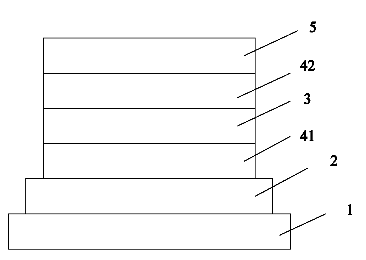
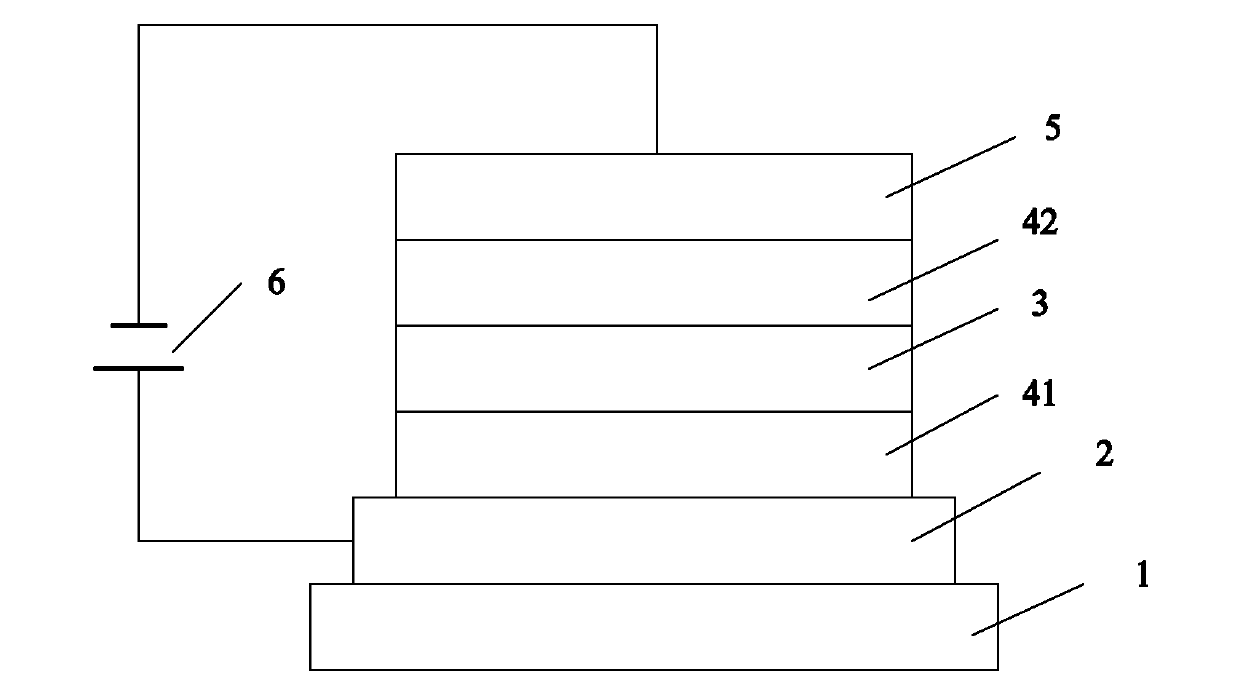
[0050] The preparation method of the organic light emitting diode provided by the present invention is

[0051] The substrate is first dried, and an anode material is used to photolithography electrodes on the dried substrate to obtain a first electrode, that is, an anode, and the anode material is indium tin oxide. Then an organic semiconductor heterojunction unit, a light emitting unit and a second electrode are sequentially formed on the first electrode. The forming method is preferably vacuum evaporation, photolithography or sputtering, and vacuum evaporation is preferably used in the present invention, because vacuum evaporation can prepare each unit with uniform thickness and very thin. In the present invention, the substrate containing the first electrode is placed in a vacuum evaporator, and an organic semiconductor heterojunction unit, a light-emitting unit and a second electrode are sequentially evaporated on the first electrode. The degree of vacuum in the vacuum e...

Embodiment 1

[0053] First, the anode indium tin oxide layer is photolithographically formed into thin strip electrodes, then cleaned, blown dry with nitrogen gas, treated with oxygen plasma for 2 minutes, and then transferred to the vacuum coating system until the vacuum degree reaches 5×10 -4 At Pascal, the first organic semiconductor heterojunction unit, the light emitting unit, the second organic semiconductor heterojunction unit and the cathode are sequentially vapor-deposited on the ITO anode, wherein the first organic semiconductor heterojunction unit adopts C 60 and pentacene formed by evaporation one by one; C 60The thickness of the pentacene is 20nm, and the thickness of the pentacene is 10nm; the hole injection layer in the light-emitting unit is made of MoO 3 , the thickness is 1nm; the hole transport layer is TCTA, the thickness is 70nm; the light emitting layer is (ppy) 2 Ir(acac) doped TCTA with a thickness of 20nm; the electron transport layer uses TPBi with a thickness of ...

Embodiment 2

[0060] First, the anode indium tin oxide layer is photolithographically formed into thin strip electrodes, then cleaned, blown dry with nitrogen gas, treated with oxygen plasma for 2 minutes, and then transferred to the vacuum coating system until the vacuum degree reaches 5×10 -4 At the same time, organic semiconductor heterojunction 1, light-emitting unit, organic semiconductor heterojunction 2, and cathode are sequentially deposited on the ITO anode, wherein organic semiconductor heterojunction 1 adopts C 60 and ZnPc formed by evaporation one by one; C 60 The thickness of ZnPc is 20nm, and the thickness of ZnPc is 15nm; the hole injection layer in the light-emitting unit is made of MoO 3 , the thickness is 1nm; the hole transport layer is TCTA, the thickness is 70nm; the light emitting layer is (ppy) 2 Ir(acac) doped TCTA with a thickness of 20nm; the electron transport layer uses TPBi with a thickness of 40nm; the electron injection layer uses Li 2 CO 3 , with a thickne...


PUM

PropertyMeasurementUnit
thicknessaaaaaaaaaa
thicknessaaaaaaaaaa
thicknessaaaaaaaaaa

Abstract

The invention provides an organic light emitting diode, wherein organic semiconductor heterojunction is arranged on the surface of an electrode; because the semiconductor heterojunction is a system which is rich in holes and electronic current carriers, thus a layer of injection and transmission unit of electrons and / or holes is equivalently increased on the surface of the electrode; and the ohm injection of the electrons and the holes is realized, thereby avoiding the unbalance injection of the electrons and / or the holes because of the inappropriate work function selection of a metal electrode, thus the luminous efficiency of the organic light emitting diode can be improved. Furthermore, because the injection efficiency of the current carriers is improved, the damage to the metal electrode is reduced and the service life is prolonged.

Description

technical field [0001] The invention relates to the technical field of organic semiconductors, in particular to an organic light emitting diode. Background technique [0002] Organic light-emitting diode display is regarded as the most popular emerging display technology in the flat panel display industry, and has been extensively researched. Compared with inorganic light-emitting diodes, organic light-emitting diodes have a wide range of material selection, can realize full-color display from blue light area to red light area, low driving voltage, high luminous brightness and luminous efficiency, wide viewing angle, fast response speed, and manufacturing process. It has many advantages such as simplicity, low cost, and easy realization of large area and flexible display, so it has developed rapidly in the past 20 years. At present, the research on organic light-emitting diodes has long been limited to academia. Almost all internationally renowned electronic companies and c...

Claims


Application Information

Patent Timeline
Patent Type & Authority Applications(China)
IPC IPC(8): H01L51/50H01L51/54H01L51/56C09K11/06
Inventor 马东阁陈永华闫东航王利祥
Owner CHANGCHUN INST OF APPLIED CHEMISTRY - CHINESE ACAD OF SCI
Why Eureka
Try Eureka