Microfluidic chip preparation method capable of realizing microsphere discretization

A microfluidic chip and discretization technology, which is applied in the photoplate making process of patterned surface, manufacturing tools, welding equipment, etc., can solve the problems of high cost, temperature, and high electric field intensity, and achieve the effect of less investment and simple process

Inactive Publication Date: 2011-09-21
CHINA NAT ACAD NANOTECH & ENG
View PDF0 Cites 34 Cited by
  • Summary
  • Abstract
  • Description
  • Claims
  • Application Information

AI Technical Summary

Problems solved by technology

However, the electric field strength required in the experiment is often very high, which can reach 0.1-10kV / mm, which will inevitably lead to higher costs and temperatures.

Method used


Image

  • Microfluidic chip preparation method capable of realizing microsphere discretization
  • Microfluidic chip preparation method capable of realizing microsphere discretization
  • Microfluidic chip preparation method capable of realizing microsphere discretization

Examples


Embodiment

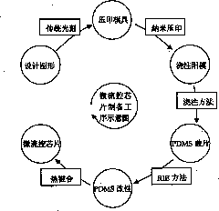
[0024] Embodiment: A kind of microfluidic chip preparation method that realizes microsphere discretization according to the present invention comprises the following steps (see figure 1 , Figure 4 ):

[0025] ① Use the IntelliMask module in the MEMS special design software IntelliSuite simulation software to design the layout for plate making, and hang-coat the photoresist (positive resist used in the experiment) on the two-inch silicon wafer with a thickness of 1 μm.

[0026]②Place the silicon wafer coated with photoresist in a vacuum drying oven for 10 minutes before drying at a temperature of 90°C. Photolithography was performed with extreme ultraviolet light, the exposure time was 8s, and then developed in a NaOH solution with a concentration of 0.6% for 40s, and the developed silicon wafer was post-baked and pre-baked for 15 minutes at a temperature of 120°C.

[0027] ③Use Oxford Plasmalab 80plus reactive ion etching machine to adjust the residual glue thickness after...


PUM

PropertyMeasurementUnit
thicknessaaaaaaaaaa

Abstract

The invention discloses a microfluidic chip preparation method capable of realizing microsphere discretization, comprising the following steps: manufacture of microfluidic chip die: manufacturing a glass-base metal mask plate to obtain a microfluidic chip pattern, transferring the pattern to a substrate which is spin-coated with photoresist by photoetching, and obtaining the microfluidic chip die with a cylindrical pattern on the substrate by dry etching; preparation of polydimethylsiloxane (PDMS) microfluidic chip substrate: polymerizing molten PDMS in situ in the convex microfluidic chip die, curing, and stripping to obtain a PDMS substrate with the pattern; and bonding of glass cover plate and PDMS substrate: etching the glass cover plate and the PDMS substrate by O2 reaction ions, and aligning and sealing the glass cover plate and the PDMS substrate. The preparation method has the advantages that the microfluidic chip prepared on the basis of the nanometer hot stamping method can be used for manufacturing casting male dies with higher bench height only by stamping the die once. The method has the advantages of low investment and simple process.

Description

(1) Technical field: [0001] The invention relates to the preparation and application of a microfluidic chip, in particular to a method for preparing a microfluidic chip that realizes the discretization of microspheres. (two) background technology: [0002] At present, with the research and development of microfluidic chips, its application fields are not limited to the fields of biochemistry and biomedicine, and it has gradually penetrated into clinical, pharmaceutical, food and environmental health monitoring and other fields. Microfluidic chips are expected to replace the functions of conventional laboratories. Through the integration and miniaturization of the analysis process, the "personalization" and "home use" of microfluidic chips will eventually be realized. Therefore, the practical application of its research is only a matter of time. question. It has only been more than ten years since the advent of microfluidic chips. At present, commercial glass chips have appe...

Claims


Application Information

Patent Timeline
Patent Type & Authority Applications(China)
IPC IPC(8): B81C1/00B81C3/00
Inventor 高鹏牟诗城徐超吴元庆屈怀泊
Owner CHINA NAT ACAD NANOTECH & ENG
Why Eureka
Try Eureka