Surface passivation method for germanium-based MOS (Metal Oxide Semiconductor) device substrate

A MOS device and substrate surface technology, which is applied in semiconductor/solid-state device manufacturing, electrical components, metal material coating technology, etc., can solve problems such as interface state density increase, defects, and gate dielectric quality deterioration, and reduce the Effects of interface state density, diffusion suppression, and passivation efficiency enhancement

Active Publication Date: 2011-10-05
SEMICONDUCTOR MANUFACTURING INTERNATIONAL (BEIJING) CORP +1
View PDF4 Cites 13 Cited by
  • Summary
  • Abstract
  • Description
  • Claims
  • Application Information

AI Technical Summary

Problems solved by technology

However, direct deposition of a high-K gate dielectric on a germanium substrate will cause the following problems: 1) The surface of the germanium substrate will be oxidized in an atmosphere with oxygen atoms, which may form volatile GeO and diffuse into the gate dielectric, A large number of dangling bonds are left at the interface between the germanium substrate and the gate dielectric, resulting in a substantial increase in the interface state density; 2) germanium diffused into the high-K gate dielectric will introduce defects in the gate dielectric, resulting in a change in the quality of the gate dielectric Difference

Method used


Image

  • Surface passivation method for germanium-based MOS (Metal Oxide Semiconductor) device substrate
  • Surface passivation method for germanium-based MOS (Metal Oxide Semiconductor) device substrate
  • Surface passivation method for germanium-based MOS (Metal Oxide Semiconductor) device substrate

Examples


Embodiment Construction

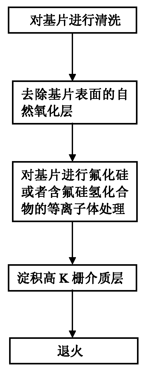
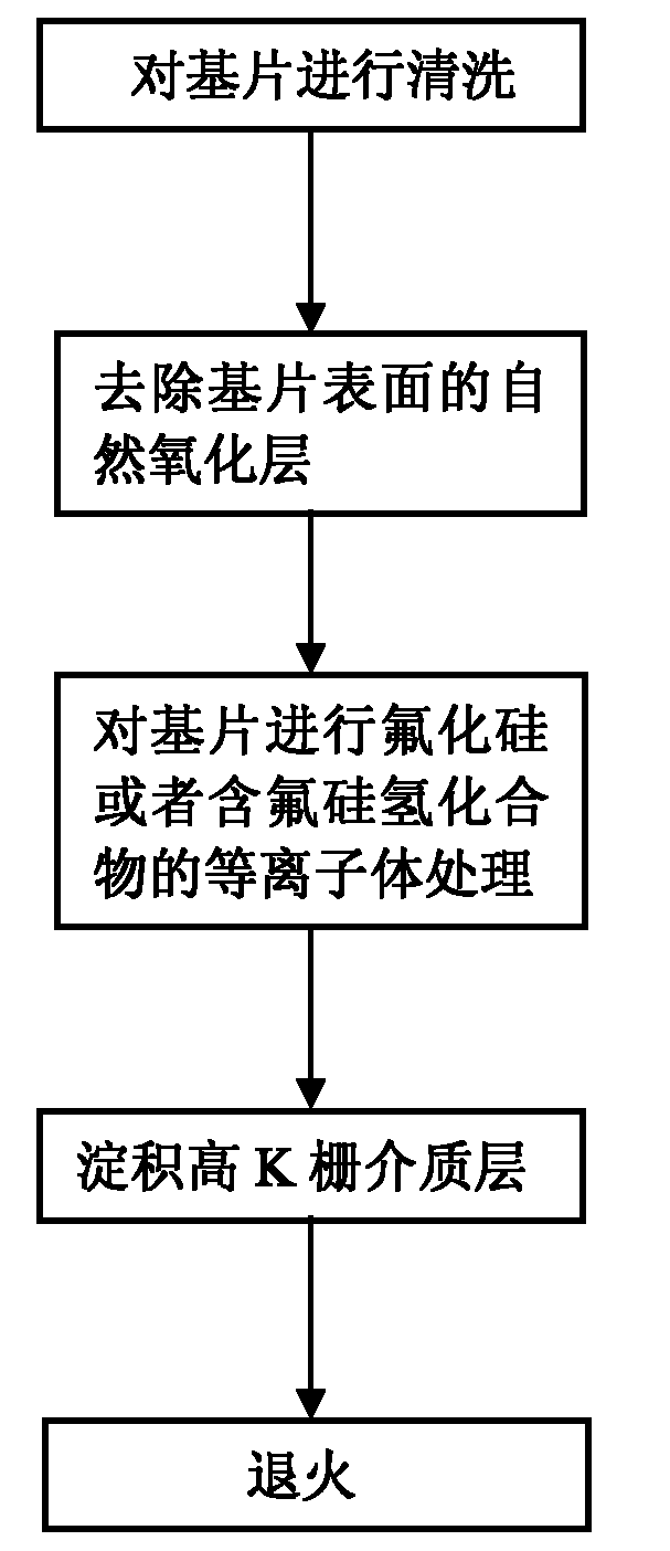
[0026] The method of the present invention will be further described through specific embodiments below in conjunction with the accompanying drawings.

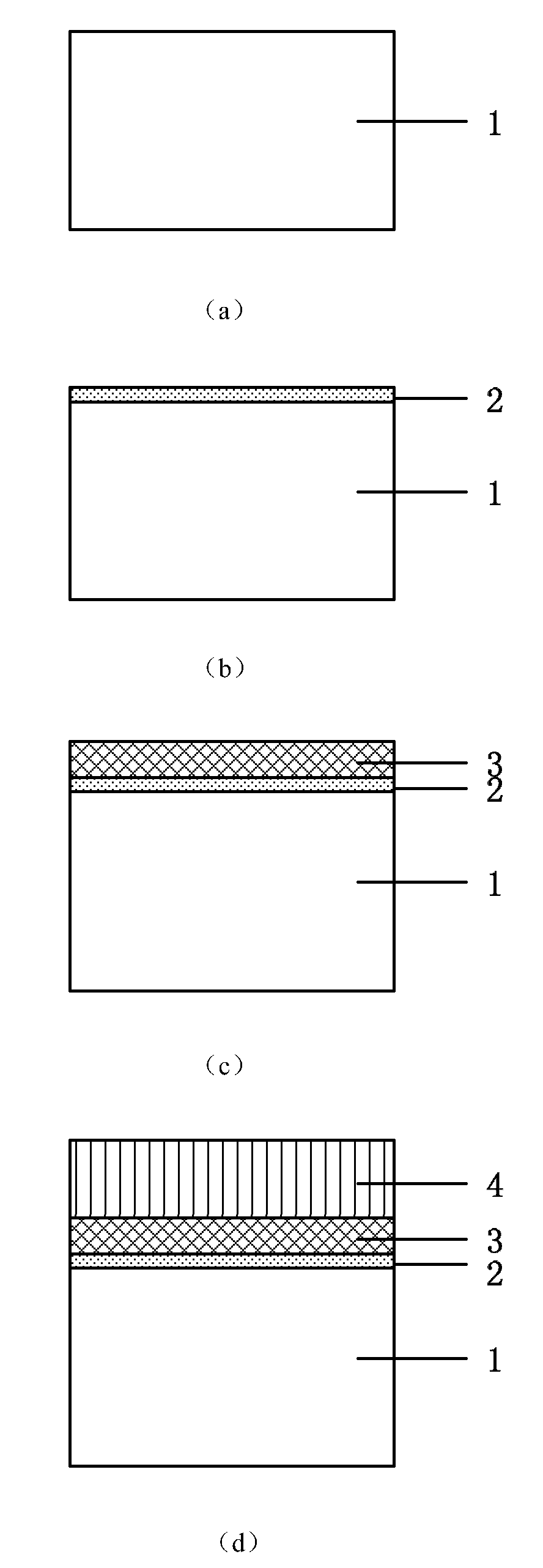
[0027] Step 1. Select a semiconductor germanium substrate, which can be a bulk germanium substrate, a GeOI (Germanium on Insulator) substrate, or epitaxial germanium (Germanium-on-silicon) on silicon, etc. The preferred example of this embodiment is a bulk germanium substrate, such as figure 2 as shown in (a);

[0028] Step 2. Cleaning the germanium substrate. First, the germanium substrate is organically cleaned, soaked and cleaned with acetone and ethanol in turn, and then rinsed with DI water to remove oil and organic pollutants on the germanium substrate. Then wash with hydrochloric acid, heat and boil in dilute hydrochloric acid, and then rinse with DI water to remove inorganic pollutants, metal particles, etc.;

[0029] Step 3. Removing the oxide on the surface of the germanium substrate. The method of soaking in HF ...


PUM


Abstract

The invention discloses a surface passivation method for a germanium-based MOS device substrate, which belongs to the field of semiconductor material devices. The method comprises the steps of: firstly, washing a semiconductor germanium substrate which is used as a substrate for removing organic, inorganic and metallic granular contaminations on a surface and removing an autoxidation layer on thesurface of the substrate; performing plasma treatment on the substrate through use of silicon fluoride or silicone and fluorin containing hydrogen compound for depositing a silicon passivation layer on the substrate; and finally, after depositing a layer of high-k gate dielectric material, and annealing. The surface passivation method disclosed by the invention has the advantages of greatly reducing the density of an interface state between interfaces of the germanium substrate and the gate dielectric material, effectively restraining the diffusion of the germanium in the substrate into the gate dielectric material, and obviously enhancing the passivation efficiency.

Description

technical field [0001] The invention belongs to the field of semiconductor material devices, and in particular relates to a method for passivating the surface of a germanium-based MOS device substrate. Background technique [0002] With the wide application of integrated circuits, the working speed of integrated circuits has become the focus of attention. In the past few decades, reducing the size of devices has been the main method to increase the speed and integration of circuits. However, as the feature size of the device shrinks to the nanoscale, traditional silicon-based transistors gradually reach the dual limits of physics and technology. In order to further increase the working speed of integrated circuits, new materials and device structures must be found. Germanium has attracted much attention due to its high electron and hole mobility. At room temperature (300K), the electron mobility of the germanium channel is 2.4 times that of silicon, and the hole mobility ...

Claims


Application Information

Patent Timeline
Patent Type & Authority Applications(China)
IPC IPC(8): C23C10/08H01L21/334
Inventor 安霞黄如林猛郭岳李志强张兴
Owner SEMICONDUCTOR MANUFACTURING INTERNATIONAL (BEIJING) CORP
Why Eureka
Try Eureka