Hetero-junction-structured crystalline silicon solar cell with intrinsic layer and preparation method thereof

A technology of solar cells and heterojunctions, applied in circuits, photovoltaic power generation, electrical components, etc., can solve problems such as unstable passivation performance, achieve the effect of reducing the surface recombination rate and ensuring stability

Inactive Publication Date: 2011-10-19
SHANGHAI INST OF TECHNICAL PHYSICS - CHINESE ACAD OF SCI
View PDF3 Cites 10 Cited by
  • Summary
  • Abstract
  • Description
  • Claims
  • Application Information

AI Technical Summary

Problems solved by technology

[0002] At present, the HIT structure crystalline silicon solar cells use amorphous silicon as the intrinsic layer to passivate the silicon surface. However, amorphous silicon has a strong absorption of short-wavelength light, and the passivation performance of silicon is not stable under UV.

Method used


Image

  • Hetero-junction-structured crystalline silicon solar cell with intrinsic layer and preparation method thereof
  • Hetero-junction-structured crystalline silicon solar cell with intrinsic layer and preparation method thereof
  • Hetero-junction-structured crystalline silicon solar cell with intrinsic layer and preparation method thereof

Examples


Embodiment

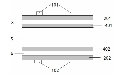
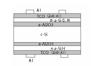
[0026] Such as figure 2 Shown, the HIT structure solar cell structure with the intrinsic layer of amorphous alumina. Its preparation process is as follows:

[0027] 1. Use the general single crystal silicon cleaning method, that is, sodium hydroxide + isopropanol (NaOH + IPA) solution to remove the surface damage of P-type CZ silicon and make texture to form an anti-reflection structure and chemical cleaning; P-type CZ silicon wafer 125 monocrystalline silicon wafers for industrial use, with a resistivity of 0.5-5 Ωcm and a thickness of 180-220um;

[0028] 2. Wash the silicon wafer obtained above with a volume ratio of HF:HCl:H2O=2:5:50 for 1 minute and then dry it, and use an atomic layer deposition (ALD) system to simultaneously prepare 5nm amorphous alumina on the upper and lower surfaces layer;

[0029] 3 Anneal the silicon wafer after depositing aluminum oxide in a nitrogen atmosphere for 15 minutes, and the annealing temperature is 425°C;

[0030] 4. Use industrial ...


PUM

PropertyMeasurementUnit
thicknessaaaaaaaaaa
thicknessaaaaaaaaaa
thicknessaaaaaaaaaa

Abstract

The invention discloses a hetero-junction-structured crystalline silicon solar cell with an intrinsic layer and a preparation method thereof. The crystalline silicon solar cell comprises a crystalline silicon substrate, and upper and lower amorphous alumina passivation dielectric layers; a p-type doped amorphous silicon carbon film and a TCO (Transparent Conductive Oxide) layer are arranged on the amorphous alumina passivation dielectric layer on the upper surface; an n-type doped amorphous silicon or micro-crystalline silicon film and a TCO layer are arranged below the amorphous alumina passivation dielectric layer on the lower surface; and the TCO layers on the upper and lower surfaces are both connected with a metal gate electrode. The preparation method comprises the steps of preparing the amorphous alumina passivation dielectric layers: preparing the ultra-thin amorphous alumina passivation dielectric layers simultaneously after the crystalline silicon substrate is acidized; and then preparing the p-type amorphous silicon carbon and the n-type amorphous silicon or micro-crystalline silicon and the TCO respectively to form the hetero-junction cell. The hetero-junction-structured crystalline silicon solar cell and the preparation method thereof have the advantages of simple process, good surface passivation performance of the crystalline silicon, good UV (ultraviolet) radiation-resistant performance, fully utilization of the sunlight and the like.

Description

technical field [0001] The invention relates to a crystalline silicon solar cell, in particular to a solar cell with a heterojunction (HIT) structure with an intrinsic layer on the surface of an amorphous aluminum oxide passivated silicon and a preparation method thereof. Background technique [0002] At present, the HIT structure crystalline silicon solar cell uses amorphous silicon as the intrinsic layer to passivate the silicon surface. However, amorphous silicon has a strong absorption of short-wavelength light, and the passivation performance of silicon is not stable under UV. The present invention adopts the amorphous aluminum oxide prepared by the atomic layer deposition (ALD) system as the intrinsic layer, which can well solve these two problems. Amorphous silicon alumina has a band gap of about 6.8eV, is completely transparent to sunlight, has good passivation performance on the silicon surface, and is not affected by UV radiation, making the battery performance mor...

Claims


Application Information

Patent Timeline
Patent Type & Authority Applications(China)
IPC IPC(8): H01L31/0216H01L31/072H01L31/18
CPCY02E10/50Y02P70/50
Inventor 褚君浩窦亚楠何悦王永谦马晓光
Owner SHANGHAI INST OF TECHNICAL PHYSICS - CHINESE ACAD OF SCI
Why Eureka
Try Eureka