Light-emitting diode with transparent electrode and preparation method

A technology of light emitting diodes and transparent electrodes, applied in circuits, electrical components, semiconductor devices, etc., can solve the problems of increasing thin film resistance, reducing light transmittance, and large operating voltage, reducing contact resistivity and improving light transmittance. efficiency, prolonging the service life

Active Publication Date: 2011-11-23
XIANGNENG HUALEI OPTOELECTRONICS
View PDF5 Cites 8 Cited by
  • Summary
  • Abstract
  • Description
  • Claims
  • Application Information

AI Technical Summary

Problems solved by technology

[0005] But in order to further increase the transmittance of its visible light region, to improve the light transmittance, it must be made into an extremely thin film, but when the nickel / gold alloy metal film is prepared as a rather thin film (about 100A ), it is easy to form an island-like discontinuous film on the surface of the gallium nitride diode, which increases the resistance of the film, and when the island-shaped film becomes larger, the light transmittance will also decrease due to the scattering effect
[0006] In addition, indium tin oxide is selected as the transparent conductive film. Compared with nickel / gold alloy metal, indium tin oxide is an N-type material, although its transmittance can reach more than 90%, but its contact resistivity is relatively high, and the operating voltage is relatively high. larger
This reduces the lifetime of the LED

Method used


Image

  • Light-emitting diode with transparent electrode and preparation method
  • Light-emitting diode with transparent electrode and preparation method
  • Light-emitting diode with transparent electrode and preparation method

Examples


preparation example Construction

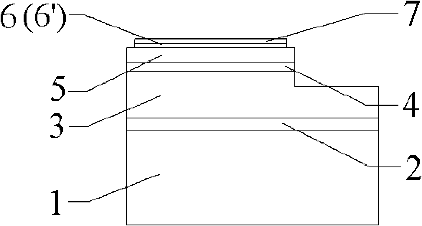
[0034] At the same time, in a typical embodiment of the present invention, a method for preparing a transparent electrode light-emitting diode is also provided, which includes a method for preparing a gallium nitride epitaxial wafer, and the method for preparing a gallium nitride epitaxial wafer includes the following steps: Growing a P-type gallium nitride layer 5; preparing a titanium layer 6 or a titanium oxide layer 6' on the P-type gallium nitride layer 5; preparing a zinc oxide layer 7 on the titanium layer 6 or the titanium oxide layer 6' to form a titanium / oxide layer Zinc or titanium oxide / zinc oxide composite transparent conductive film.

[0035] A specific preparation method for preparing a titanium / zinc oxide composite transparent conductive film and a titanium oxide / zinc oxide composite transparent conductive film is respectively given as follows.

[0036] Wherein, in the step of preparing the titanium / zinc oxide composite transparent conductive film, the step of ...
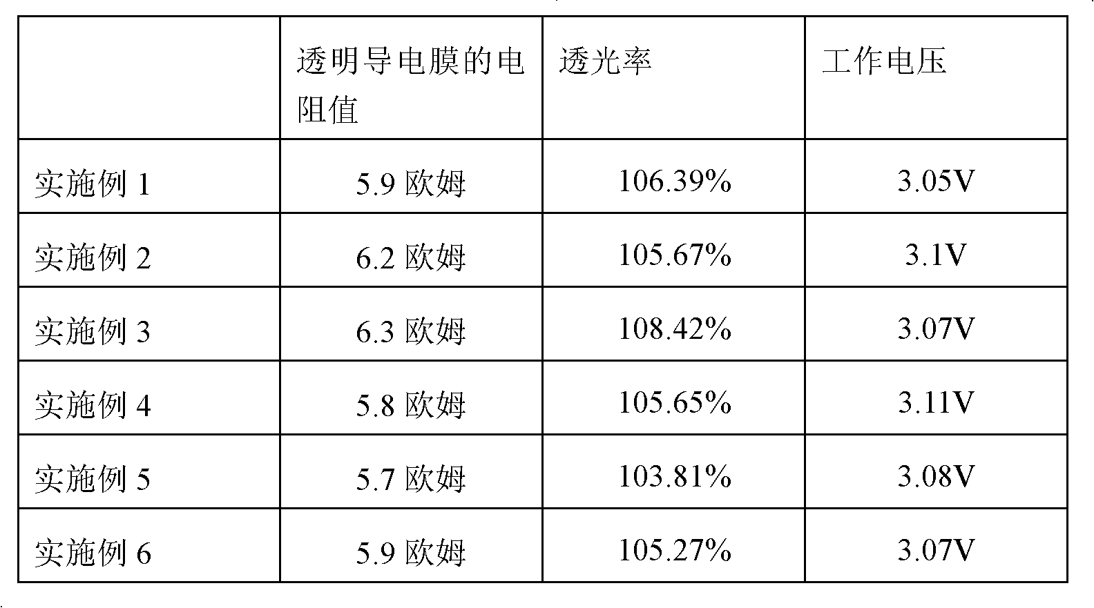
Embodiment 1

[0044] The specific operation steps are as follows:

[0045] 1. High temperature treatment: In the MOCVD reaction chamber, high-purity H 2 , reduce the pressure of the reaction chamber to 150mbar, heat the 0001-face sapphire 1 to 1100°C, and treat at high temperature for 5 minutes to 20 minutes.

[0046] 2. Nitriding treatment: reduce the temperature to 500°C, and use NH with a flow rate of 8 standard liters / minute 3 It is passed into the reaction chamber and maintained for 120 seconds to perform nitriding treatment on the sapphire substrate 1 .

[0047] 3. Growth of low-temperature buffer gallium nitride layer 2: reduce the temperature to 500°C, increase the pressure to 600mbar, and 2 Under the atmosphere, NH with a flow rate of 8 standard liters / min 3 , the flow rate is 3.8×10 -4 TMGa per mol / min, H2 at a flow rate of 80 standard liters / min, and a low-temperature buffer gallium nitride layer 2 with a thickness of 30 nanometers grown on a sapphire substrate.

[0048] 4. ...

Embodiment 2

[0055] Preparation method: steps 1-6 are the same as in Example 1, and step 7 is as follows:

[0056] Preparation of titanium / zinc oxide composite transparent conductive film: at room temperature, greater than 10 -7 Under the vacuum degree of Torr, the titanium layer 6 of 25 angstroms is formed by vacuum evaporation using an electron beam evaporation machine; after the titanium layer 6 is formed, the temperature is raised to 500 ° C, and the heat treatment is carried out in an atmosphere with a volume ratio of nitrogen and oxygen of 10:40. The titanium layer 6 forms a surface protection layer; in the environment where the volume ratio of 38% hydrochloric acid and 65% nitric acid is 3:1, the wet etching titanium layer 6 forms a first through hole with a diameter of 1.5 microns; The temperature is adjusted to 200°C, and the oxygen flow rate is 8 sccm, greater than 10 -6 Under the vacuum degree of Torr, use an oxide evaporation machine to vacuum vapor-deposit to form a 3000 angs...


PUM

PropertyMeasurementUnit
thicknessaaaaaaaaaa
thicknessaaaaaaaaaa
thicknessaaaaaaaaaa

Abstract

The invention discloses a light-emitting diode with a transparent electrode and a preparation method. The light-emitting diode with the transparent electrode comprises a gallium nitride epitaxial wafer. In the gallium nitride epitaxial wafer, a transparent conductive film layer is covered on a P-type gallium nitride layer, and is a titanium/zinc oxide or titanium oxide/zinc oxide composite transparent conductive film. The titanium/zinc oxide composite transparent conductive film comprises a titanium layer covered on the P-type gallium nitride layer and a zinc oxide layer covered on the titanium layer. The titanium oxide/zinc oxide composite transparent conductive film comprises a titanium oxide layer covered on the P-type gallium nitride layer and the zinc oxide layer covered on the titanium oxide layer. In the light-emitting diode with the transparent electrode, the material of the transparent conductive film layer on the P-type gallium nitride layer in the gallium nitride epitaxial wafer of the diode is improved to reduce the contact resistivity of the transparent conductive film layer, improve light transmittance and the luminous efficiency of the light-emitting diode with the transparent electrode and prolong the service life of the light-emitting diode with the transparent electrode.

Description

technical field [0001] The invention relates to the application field of diodes, in particular to a transparent electrode light-emitting diode and a preparation method thereof. Background technique [0002] The light-emitting diode includes gallium nitride epitaxial wafers and packages wrapped outside the epitaxial wafers. Since the gallium nitride material has a direct energy gap and its energy gap is wide (about 3.4eV at room temperature), it is a It is a raw material that is very suitable for preparing blue and green light-emitting material elements. In the process of growing gallium nitride epitaxial wafers by MOCVD, the concentration of the P-type gallium nitride epitaxial layer has been unable to increase to the level compared with that of N-type gallium nitride, and the use of MOCVD (metal organic chemical vapor phase epitaxy system) during epitaxy growth, NH 3 The released H atoms form a recombination center with Mg, and the deep energy level to which the recombina...

Claims


Application Information

Patent Timeline
Patent Type & Authority Applications(China)
IPC IPC(8): H01L33/42H01L33/00
Inventor 谈健徐亚兵岑龙斌
Owner XIANGNENG HUALEI OPTOELECTRONICS
Why Eureka
Try Eureka