A high-density array chip device and application for digital nucleic acid amplification
A nucleic acid and chip technology, applied in the field of detection devices in many fields, can solve the problems of unfavorable preparation methods and application costs, difficulty in entering ordinary laboratories, expensive chips and supporting instruments, etc., to reduce experimental costs, prevent external pollution, The effect of preventing cross-contamination
- Summary
- Abstract
- Description
- Claims
- Application Information
AI Technical Summary
Problems solved by technology
Method used
Image
Examples
Embodiment 1
[0034] Example 1 High-density glass chip device for digital nucleic acid amplification
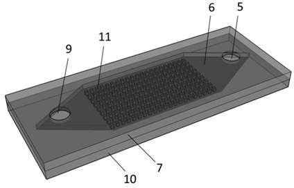
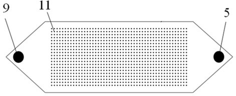
[0035] Referring to Figures 1-3, an integrated flow chip device for digital nucleic acid amplification is composed of a vacuum system 1, a pipeline 2, a suction cup 3, a capping layer 7 and a reaction layer 10, and the capping layer 7 and the reaction layer After the layers 10 are sealed, an integrated flow path chip assembly is formed. The two ends of the capping layer 7 are provided with a sample inlet 9 and a sample outlet 5. The reverse side of the capping layer 7 is an irregular hexagonal concave surface. When the capping layer After 7 is sealed with the reaction layer 10, the channel 6 is formed. The reaction layer 10 is provided with high-density integrated reaction chambers 11 arranged in a matrix. The vacuum system 1 is connected to the suction cup 3 through the pipeline 2, and the suction cup 3 is placed on the cover layer 7 for sampling. On the port 5, the sample outlet 5 is con...
Embodiment 2
[0041] Example 2 High-density monocrystalline silicon chip device for digital nucleic acid amplification
[0042] The structure of the device is the same as in Example 1.
[0043] The reaction layer 10 is made of a polished single-crystal silicon wafer with a thickness of 500 μm, and the reaction chamber 11 is formed by photolithography and chemical wet etching. The reaction chamber 11 is a square with a side length of 100 μm, 200 μm or 300 μm, and a depth of 50 μm, 100 μm, 200 μm, 300 μm. According to different widths and etching depths, the volume of the reaction chamber 11 can be 500 pL, 1 nL, 2 nL, 4.5 nL, 8 nL, 9 nL, 18 nL; the reaction chamber 11 can also be pentagonal, rhombus, circular shape or other polygons.
[0044] The cover layer 7 can be made of glass or a transparent PMMA plate according to different applications. Use standard photolithography and etching techniques to form an irregular hexagonal concave surface on the reverse side of the capping layer 7, wit...
Embodiment 3
[0049] Example 3 Digital-Loop Mediated Isothermal Amplification (Digital-Loop Mediated Isothermal Amplification, Digital-LAMP)
[0050] The device of Example 1 is used to inject samples, and then perform subsequent digital nucleic acid loop-mediated isothermal amplification.
[0051] Specific steps:
[0052] 1. The channel structure is the same as that in Embodiment 1, and the designed structure is printed onto film with an inkjet printer as a mask for photolithography.
[0053] 2. The reaction layer 10 is made of glass with a thickness of 1 mm, and the reaction chamber 11 is made by standard photolithography and etching technology. The reaction chamber 11 is a square with a side length of 100 μm, 200 μm or 300 μm, and a depth of 50 μm or 100 μm. or 200 μm; according to different widths and etching depths, the volume of the reaction chamber 11 can be 500 pL, 1 nL, 2 nL, 4.5 nL, 8 nL, 9 nL or 18nL; the reaction chamber 11 can also be pentagonal, Rhombus or circle.
[0054] 3...
PUM
 Abstract
Description
Claims
Application Information


