
Passivation process for back of crystalline silicon solar cell and structure of back-passivated crystalline silicon solar cell

A solar cell, crystalline silicon technology, applied in circuits, photovoltaic power generation, electrical components, etc., can solve problems such as destroying passivation effects, and achieve the effects of reducing series resistance, protecting alumina, and reducing surface recombination rate

Inactive Publication Date: 2012-03-14
TRINA SOLAR CO LTD
View PDF4 Cites 9 Cited by
  • Summary
  • Abstract
  • Description
  • Claims
  • Application Information

AI Technical Summary

Problems solved by technology

[0003] These processes of depositing dielectric films, opening holes with corrosive paste, and printing aluminum paste for sintering all have a common problem. The sintering process often destroys the passivation effect.

Method used


Image

  • Passivation process for back of crystalline silicon solar cell and structure of back-passivated crystalline silicon solar cell
  • Passivation process for back of crystalline silicon solar cell and structure of back-passivated crystalline silicon solar cell
  • Passivation process for back of crystalline silicon solar cell and structure of back-passivated crystalline silicon solar cell

Examples


Embodiment 1

[0028] After the P-type silicon wafer is cleaned and textured, PECVD equipment is used to coat a layer of silicon nitride film on the back surface of the silicon wafer. The slurry opens pores on the surface of the silicon nitride, the size of the pores is 300 microns in diameter and the pitch is 900 microns. The slurry is 1% to 50% ammonium hydrogen fluoride and organic matter. The drying temperature of the slurry is 250°C for 5 to 30 minutes. B re-diffusion is carried out at a certain diffusion temperature. After heavy doping is completed, the silicon nitride mask is removed with 1% to 30% hydrofluoric acid solution or 1% to 50% phosphoric acid solution, and then PECVD is used to plate 30nm on the back surface of the silicon wafer. Aluminum oxide, the coating temperature is 300-350°C; then enter the rapid annealing furnace for annealing in H2 atmosphere, the annealing temperature is 400°C, the annealing time is 15min, and then use PECVD to coat about 100nm of nitride on the b...


PUM

PropertyMeasurementUnit
thicknessaaaaaaaaaa
thicknessaaaaaaaaaa

Abstract

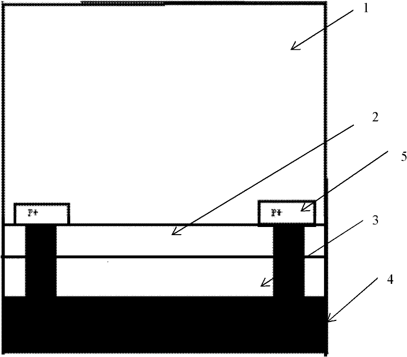
The invention relates to a passivation process for a back of a crystalline silicon solar cell and a structure of a back-passivated crystalline silicon solar cell. The passivation process comprises: firstly, based on silicon nitride used as a mask on the back of a P-type silicon wafer, forming holes on the mask, then carrying out B diffusion to form heavy doping at the hole positions, washing away the silicon nitride mask, depositing a laminated film of aluminum oxide and silicon nitride, forming back contact patterns on the back of a cell, and manufacturing an aluminum electrode on the back of the cell. The invention has the beneficial effects that: the back-passivated solar cell has the following two characteristics: (1) a high-doped heavy-diffusion region is formed at the back contact and near position thereof of the cell, and the high-doped heavy-diffusion region is in good ohmic contact with the plated aluminum electrode, thus the series resistance of the cell is reduced; and (2) by annealing aluminum oxide, the back surface can be well passivated and the surface compounding rate is reduced, and silicon nitride has an action of protecting aluminum oxide, thus the destroy of aluminum oxide passivation effect in subsequent sputtering or evaporation process is avoided.

Description

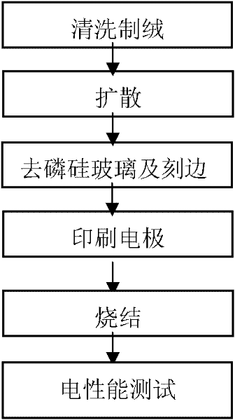
technical field [0001] The invention relates to a rear passivation process and structure of a crystalline silicon solar cell. Background technique [0002] Traditional solar cell fabrication methods, such as figure 1 As shown, the process flow is cleaning texture, diffusion, edge etching and PSG removal, PECVD SiNx film plating, screen printing, sintering and electrical performance testing. This traditional process determines that the efficiency of solar cells cannot be greatly improved, and the back passivation can reduce the surface recombination rate of the battery, which can greatly improve the efficiency. The existing methods of back passivation batteries are: 1. Backside plating Alumina is passivated, holes are opened using a corrosive paste, and then aluminum paste is printed for sintering. 2. The back is plated with silicon oxide for passivation, using corrosive paste to open holes, and then printing aluminum paste for sintering. 3. The back is plated with silicon...

Claims


Application Information

Patent Timeline
Patent Type & Authority Applications(China)
IPC IPC(8): H01L31/18H01L31/0224H01L31/0216H01L31/0236
CPCY02E10/50Y02P70/50
Inventor 王书博邓伟伟
Owner TRINA SOLAR CO LTD
Learn More