Anode material of lithium-ion battery and method for preparing anode material
A technology for lithium ion batteries and negative electrode materials, applied in battery electrodes, circuits, electrical components, etc., can solve the problems of low cycle times of amorphous silicon-based films, easy blocking of lithium ion migration channels, and poor conductivity of silicon nanowires. Achieving the effect of improved Coulombic efficiency, improved battery cycle performance, and increased concentration of conductive holes or electrons
- Summary
- Abstract
- Description
- Claims
- Application Information
AI Technical Summary
Problems solved by technology
Method used
Image
Examples
Embodiment 1
[0040] The method for preparing lithium-ion battery negative electrode material in this embodiment mainly includes the following steps:
[0041] Step 1: Take recycled P-type high-doped solar-grade crystalline silicon scraps as electrode materials, and use the SZ-82 digital four-probe tester of Suzhou Telecom Instrument Factory to measure the resistivity to 7.1Ω·cm.
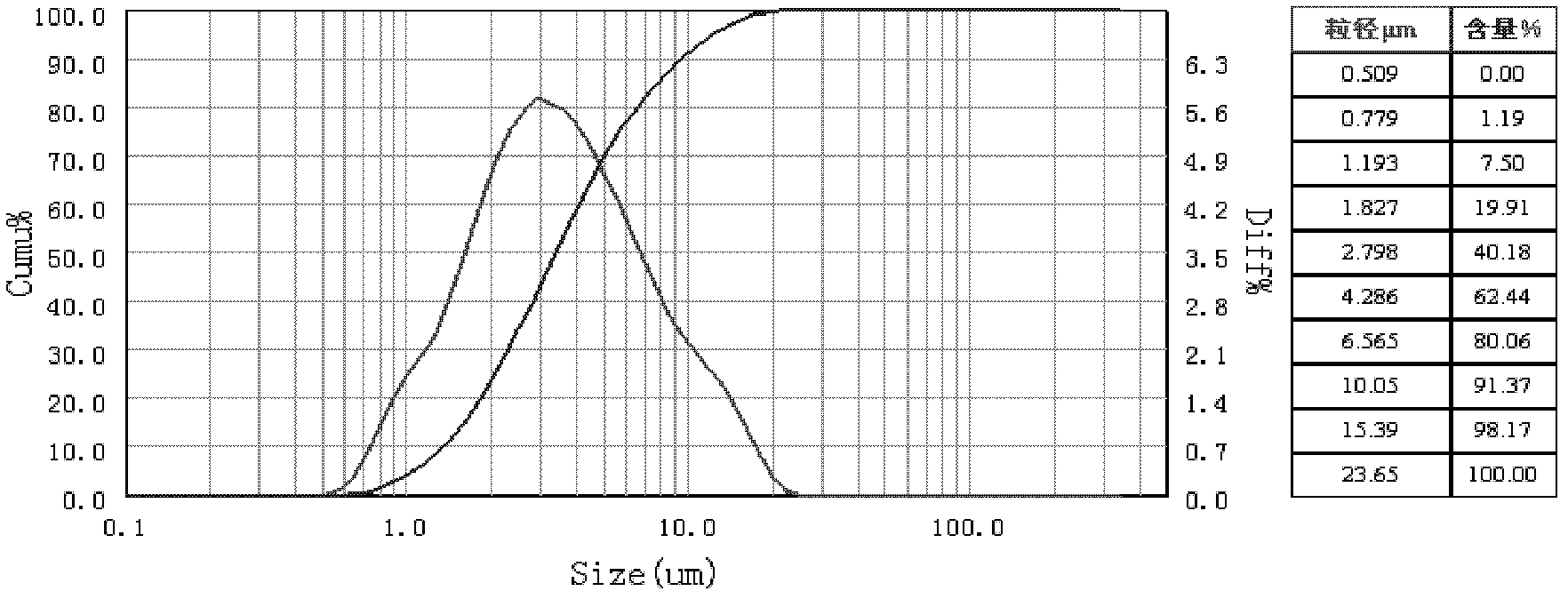
[0042] Step 2: After washing, drying and crushing P-type crystalline silicon into small particles of about 1 mm, use a star ball mill for 8 hours to obtain silicon microcrystals with a median diameter of 3.364 μm. The particle size distribution diagram is shown in figure 1 .
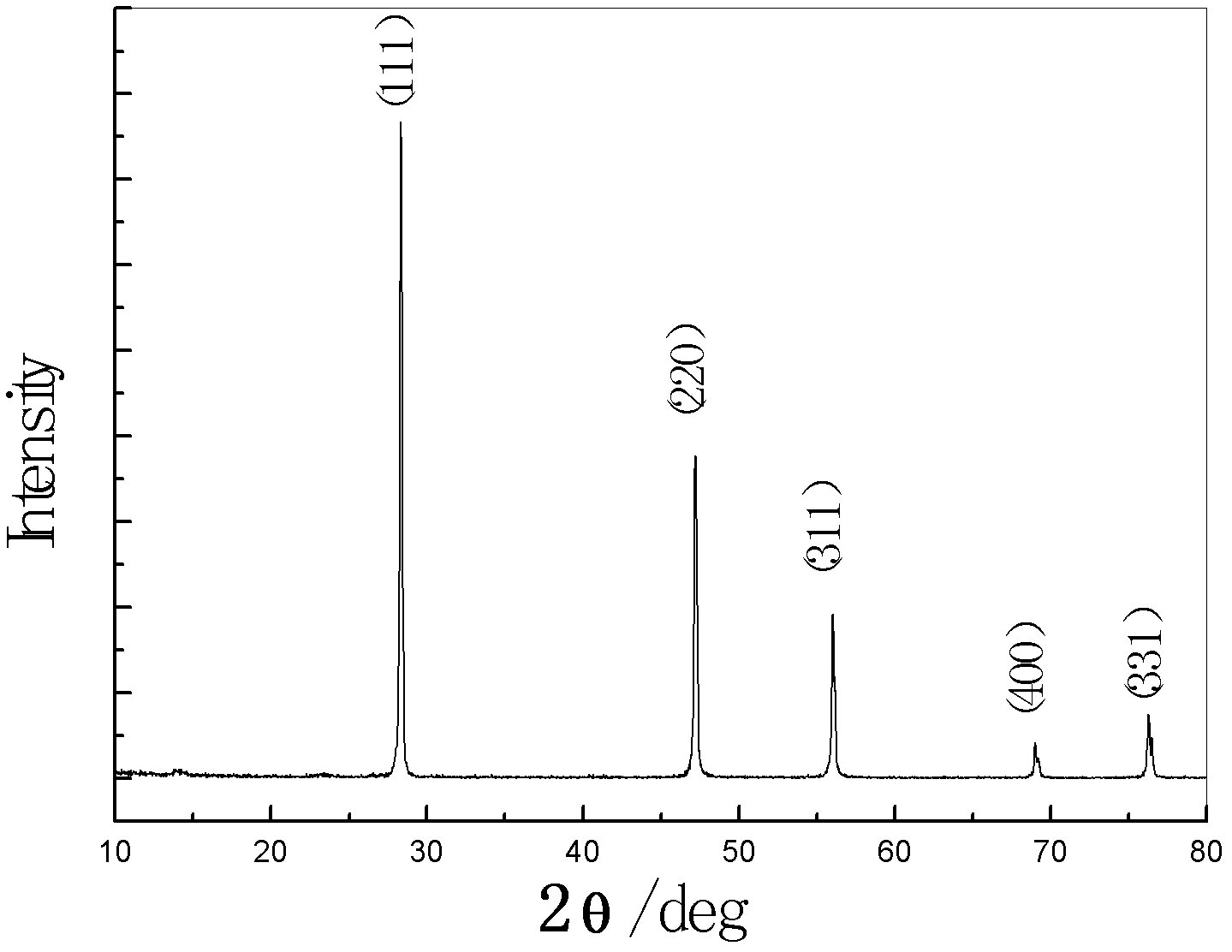
[0043] Step 3: Measure the XRD of the powder obtained in step 2 to obtain figure 2 , indicating that the main component of the silicon active material is crystalline silicon.
[0044] Step 4: Mix the above-mentioned doped crystalline silicon active powder with a mass fraction of 75%, 15% PVDF (polyvinylidene fluoride) and 10% acetylene bl...
Embodiment 2
[0047] The method for preparing lithium-ion battery negative electrode material in this embodiment mainly includes the following steps:
[0048] Step 1: Produce bulk solar-grade polysilicon by the improved Siemens method (closed-loop trichlorosilane hydrogen reduction method).
[0049] Step 2: adding a master alloy containing B element to the above silicon material, doping and casting an ingot under the conditions of vacuum and high temperature 1350-1500° C. to obtain a P-type crystalline silicon active material with a resistivity of 5.1Ω·cm.
[0050] Step 3: Wash, dry, and pulverize the P-type crystalline silicon obtained in Step 2 into small particles of about 1 mm, and then ball mill it with a star ball mill for 10 hours. The median diameter of the silicon crystal is 2.904 μm.
[0051] Step 4: Mix the doped crystalline silicon active powder obtained in step 3 with a mass fraction of 60%, 20% PVDF (polyvinylidene fluoride) and 20% acetylene black, and drop an appropriate amo...
Embodiment 3
[0054] The difference from Example 2 is that the doping of B is changed to doping of P. The obtained sample is marked as A3, and its capacity cycle performance is shown in Table 1.
PUM
| Property | Measurement | Unit |
|---|---|---|
| particle diameter | aaaaa | aaaaa |
| electrical resistivity | aaaaa | aaaaa |
| thickness | aaaaa | aaaaa |
Abstract
Description
Claims
Application Information


