
Preparation method of horizontal phase change storage irrelevant to photoetching resolution ratio

A technology of phase-change memory and lithographic resolution, applied in the field of preparation of horizontal phase-change memory, can solve the problem of large-area, high-precision, economical and efficient preparation, cannot realize efficient preparation of fine graphics, phase-change memory operation current Oversize and other problems, to achieve the effect of high preparation precision, simple structure, and improved integration

Inactive Publication Date: 2012-07-18
INST OF SEMICONDUCTORS - CHINESE ACAD OF SCI
View PDF5 Cites 6 Cited by
  • Summary
  • Abstract
  • Description
  • Claims
  • Application Information

AI Technical Summary

Problems solved by technology

At present, the main problem faced by phase change memory is that the operating current is too large and the requirements for the drive circuit are high, which limits the reduction of storage power consumption, the improvement of storage speed and the increase of storage density.
For the technical bottleneck of excessive PCRAM operating current, conventional solutions (such as the preparation of plug electrodes in vertical devices) are highly dependent on optical lithography resolution, CMP, MOCVD and other processes, and it is difficult to achieve large-area, high-precision , economical and efficient preparation
Although linear processing technologies such as electron beam exposure and focused particle beam etching with high preparation precision can achieve high preparation precision, they cannot achieve efficient preparation of fine patterns on large-area substrates due to the limitation of processing speed.

Method used


Image

  • Preparation method of horizontal phase change storage irrelevant to photoetching resolution ratio
  • Preparation method of horizontal phase change storage irrelevant to photoetching resolution ratio
  • Preparation method of horizontal phase change storage irrelevant to photoetching resolution ratio

Examples


Embodiment Construction

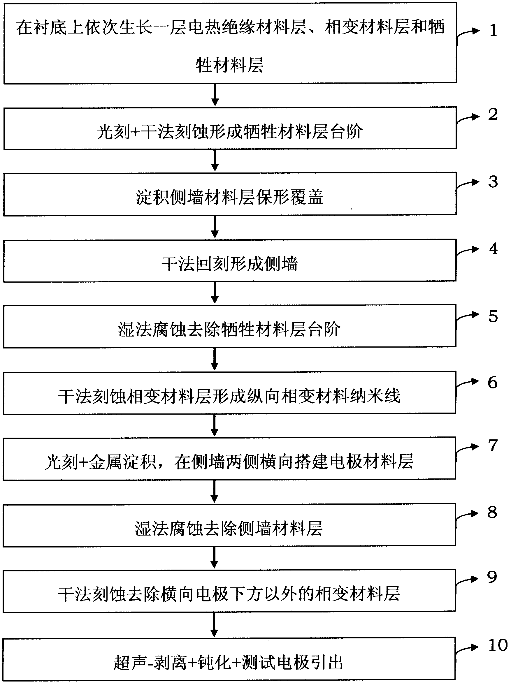
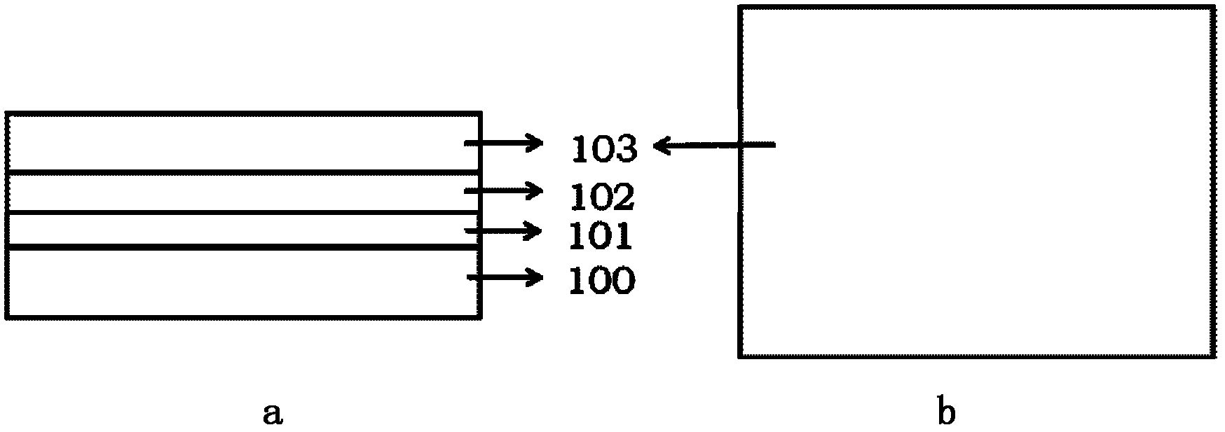
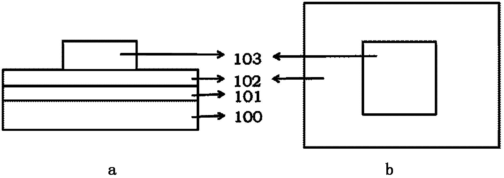
[0022] see figure 1 , see in conjunction with Figure 2 to Figure 11 As shown, the present invention provides a method for preparing a horizontal phase-change memory that has nothing to do with photolithographic resolution, the method comprising:

[0023] Step 1: grow a corrosion-resistant electrothermal insulating material layer 101 on the substrate 100, deposit a phase change material layer 102 on the electrothermal insulating material layer 101, wherein the material of the substrate 100 is silicon, gallium nitride, sapphire , silicon carbide, gallium arsenide or glass and other existing and future substrate materials. The material of the electrical insulation material layer 101 is nitrogen oxide compound, nitride or oxide, or a mixture of these compounds, and the electrical insulation material layer 101 is formed by sputtering, evaporation, chemical vapor deposition deposition method, laser-assisted deposition method, atomic layer deposition method, thermal oxidation meth...


PUM


Abstract

A preparation method of a horizontal phase change storage irrelevant to photoetching resolution ratio comprises sequentially growing an electric heating insulation material layer, a phase change material layer and a sacrifice material layer on a substrate; forming steps for preparing lateral walls through photoetching and dry etching methods; depositing on the upper surface of a shape-protection covering sample of a lateral wall material; etching a lateral wall material layer in returning mode in a dry method, removing the lateral wall material layer, forming a lateral wall with the height and the width in nanoscale; using wet etching to remove the sacrifice material layer, etching the phase change material layer in a dry method and forming a nanowire of the phase change material; preparing an anticorrosive electrode material layer at one edge of the lateral wall material layer and transversely striding a longitudinal lamination nanowire structure constructed by the sacrifice materiallayer and the lateral wall material layer; conducting wet etching to remove the lateral wall material layer; conducting dry etching to remove the phase change material layer outside the position below the electrode material layer through a metal electrode material layer mask; and peeling to form a structure that the phase change material layer is all limited between the electrode material layer, passivating and leading out a test electrode, and completing preparation of devices.

Description

technical field [0001] The invention relates to the field of micro-nano technology, in particular to a preparation method of a horizontal phase-change memory which is independent of photolithography resolution. The invention proposes a method for self-aligning and preparing a horizontal fully-confined phase-change memory device by adopting a sidewall process and an ultrasonic-stripping process. This method avoids the disadvantages of high cost and long cycle of linear lithography methods such as electron beam exposure and focused particle beam etching, and breaks through the limitation of optical lithography resolution. It is suitable for nanoscale devices on large-area substrates. Preparation has great advantages in terms of preparation accuracy, preparation efficiency, economy, and compatibility with existing CMOS processes. Background technique [0002] The accelerated development of high-tech industries and basic service facilities has higher and higher requirements for...

Claims


Application Information

Patent Timeline
IPC IPC(8): H01L45/00
Inventor 付英春王晓峰张加勇季安杨富华
Owner INST OF SEMICONDUCTORS - CHINESE ACAD OF SCI
Learn More