Method for manufacturing silicone micro-nano optical structure by using imprinting technology

An optical structure, micro-nano technology, applied in the manufacture of microstructure devices, microstructure devices, optics, etc., can solve problems such as high pressure, and achieve the effects of low transmission loss, excellent optical properties, and improved environmental resistance

Inactive Publication Date: 2012-10-03
SOUTH CHINA NORMAL UNIVERSITY
View PDF18 Cites 24 Cited by
  • Summary
  • Abstract
  • Description
  • Claims
  • Application Information

AI Technical Summary

Problems solved by technology

This technology mainly prepares a high-resolution master plate through electron beam direct writing and other devices, and then uses the imprinting method to replicate a stamper that can be reused many times, and then uses this template

Method used


Image

  • Method for manufacturing silicone micro-nano optical structure by using imprinting technology
  • Method for manufacturing silicone micro-nano optical structure by using imprinting technology
  • Method for manufacturing silicone micro-nano optical structure by using imprinting technology

Examples


Example Embodiment

[0032] Example 1

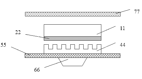
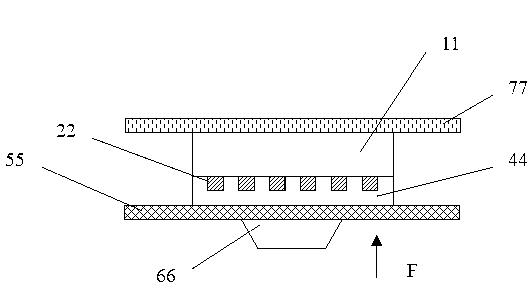
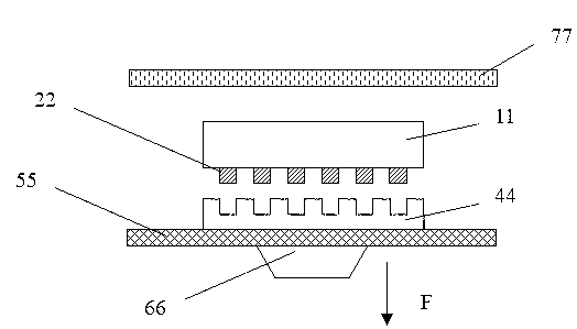
[0033] The silicone micro-nano optical structure is prepared by a hot embossing method, and the specific steps include:

[0034] 1. Use the photonic device simulation software to design and optimize the optical waveguide device, then use the computer-aided design tool to draw the layout of the mask according to the design results, and transfer the designed pattern file to the professional photolithography mask manufacturer for customization;

[0035] 2. Expose the photoresist, and then perform ICP etching to obtain a stamp of silicon or other materials for imprinting; if the minimum line width of the device is relatively high, electron beam exposure or other advanced lithography equipment can be used to customize.

[0036] 3. Hydroxylate the surface of the silicon stamp or other hard template, then place it in a petri dish in an anhydrous environment, inject an appropriate amount of perfluorotetrahydrooctylsilane with a microliter syringe, and heat it f...

Example Embodiment

[0041] Example 2

[0042] 1. Use the photonic device simulation software to design and optimize the optical waveguide device, then use the computer-aided design tool to draw the layout of the mask according to the design results, and transfer the designed pattern file to the professional photolithography mask manufacturer for customization;

[0043] 2. Expose the photoresist, and then perform ICP etching to obtain a stamp of silicon or other materials for imprinting; if the minimum line width of the device is relatively high, electron beam exposure or other advanced lithography equipment can be used to customize.

[0044] 3. Hydroxylate the surface of the silicon stamp or other hard template, then place it in a petri dish in an anhydrous environment, inject an appropriate amount of perfluorotetrahydrooctylsilane with a microliter syringe, and heat it from room temperature to 250°C After the temperature is stabilized, keep it for 2 hours. After cooling, use n-hexane to wash ...


PUM


Abstract

The invention discloses a method for manufacturing a silicone micro-nano optical structure by using an imprinting technology. Firstly, a template serving as a seal during the imprinting is designed and processed according to the requirements of the structure of a device; secondly, an appropriate substrate material is selected and used according to the requirements of the micro-nano optical structure of the device, and then covered with imprinting glue; afterwards, structural patterns on the template are transferred to the imprinting glue by adopting an imprinting process, the imprinting glue is solidified and molded, the template is released after the template and the substrate are both cooled, and then a micro-nano optical structure with embossed figures is obtained; and finally, a polymeric optical bounding layer covers above imprinted lines according to the design of the device, and then the whole micro-nano optical structure is formed. By adopting the method, optical devices whichhave good weatherability and strong thermal stability and cause low loss can be prepared; and besides, the process is simple, so that the method has a cost advantage.

Description

technical field [0001] The invention relates to the fields of embossing technology and optical technology, in particular to a method for making a silicone micro-nano optical structure by applying the embossing technology. Background technique [0002] Optical waveguides are important fundamental components of integrated optics. Optical waveguide devices can be divided into four basic types according to their composition materials: lithium niobate-plated titanium optical waveguide, silicon-based silica optical waveguide, InGaAsP / InP optical waveguide and polymer optical waveguide. Among them, the polymer optical waveguide has become a focus of attention and research due to its advantages such as low coupling loss, good optical performance, and small size. The search for a low-cost polymer optical waveguide preparation method has naturally become a subject of concern. [0003] Traditional optical waveguide devices are made on inorganic materials, such as lithium niobate and s...

Claims


Application Information

Patent Timeline
IPC IPC(8): G02B6/13G03F7/00B81C1/00
Inventor 梅霆万磊王洪朝郭克芹杜康朱凝
Owner SOUTH CHINA NORMAL UNIVERSITY
Why Eureka
Try Eureka