Preparation method of carbon microelectrode array structure
An array structure and carbon microelectrode technology, which is applied in the direction of microstructure technology, microstructure devices, and manufacturing microstructure devices, can solve the problems of generating wrinkles and not considering the preparation of nano-fold structures, and achieve fine graphics, long service life, The effect of simple process
- Summary
- Abstract
- Description
- Claims
- Application Information
AI Technical Summary
Problems solved by technology
Method used
Image
Examples
Embodiment 1
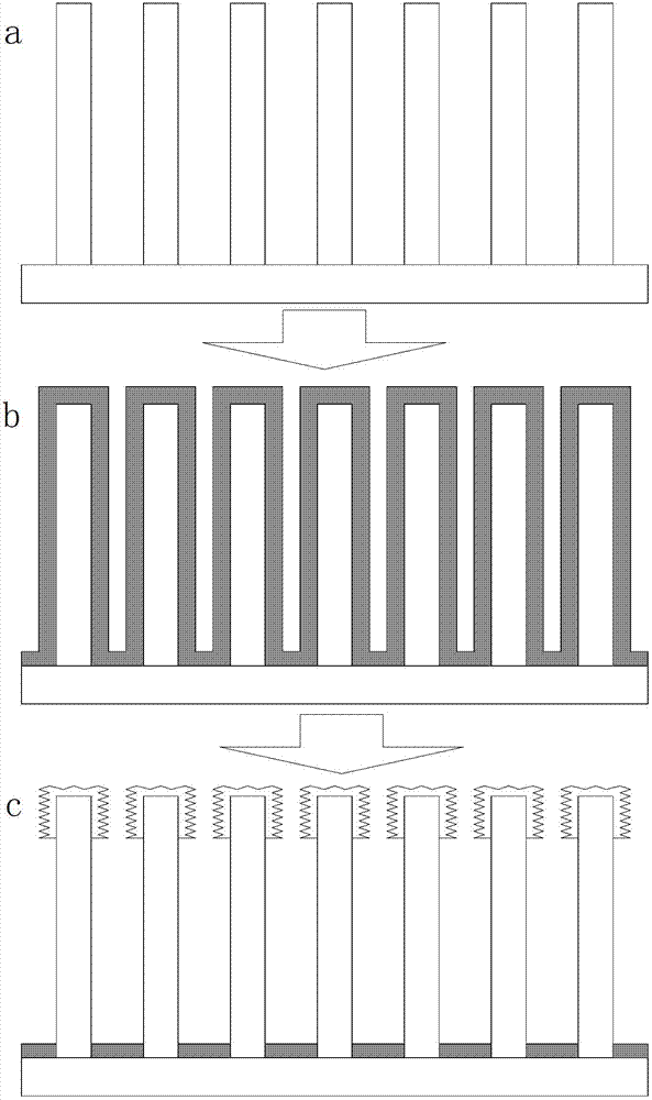
[0036] (1) Photolithography steps:
[0037] (1.1) Cleaning steps: Clean a 2-inch silicon wafer ultrasonically for 10 minutes with acetone, put it in SPM (mixed solution of concentrated sulfuric acid and hydrogen peroxide), heat and clean it at 80°C for 15 minutes, and then clean it thoroughly with deionized water Finally, place it on a 200°C hot plate and bake it for 15 minutes to make it completely dry;
[0038] (1.2) Homogenization step: Coat SU-82100 negative photoresist on the cleaned silicon substrate on the KW-4A type homogenizer (diluted with relevant diluents such as propylene glycol methyl ether acetate (PGMEA)), The homogenization is carried out in two steps. The homogenization machine first rotates at a low speed of 500r / min for 50s, and then rotates at a high speed of 1000r / min for 100s. The function is to volatilize the solvent and fix the adhesive layer to prepare for better exposure. If the pre-baking is insufficient, it will easily lead to the adhesion of the ad...
Embodiment 2
[0057] The relevant steps are the same as those in Example 1, except that in step (7), instead of depositing nickel, a layer of aluminum is deposited with a thickness of about 500 nm during metal deposition. In this embodiment, the main process parameters of one-step pyrolysis are listed in Table 3.
[0058] The one-step pyrolysis process parameter of table 3 embodiment 2
[0059]
[0060]
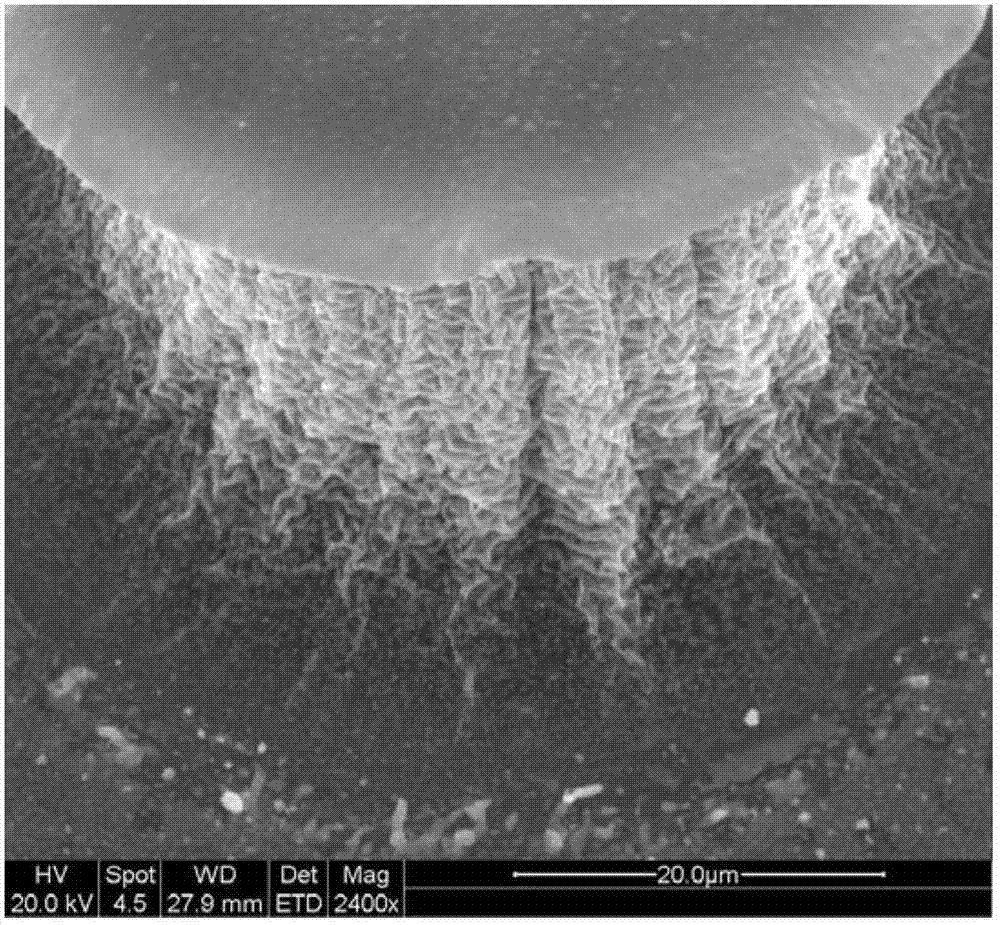
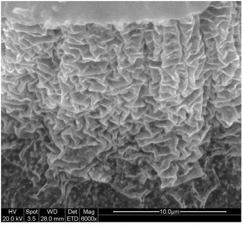
[0061] After pyrolysis, a carbon microstructure array with a large amount of integrated metal nanofold structure on the surface is also obtained, as shown in Figure 3(a) and Figure 3(b), and the metal nanofold growth site after pyrolysis is shown in Figure 3(a) As shown, the growth of metal nanofolds on carbon pillars is shown in Fig. 3(b).
Embodiment 3
[0063] The relevant steps are the same as those in Example 1, except that in step (7), when the metal is deposited, instead of depositing a single layer of metal, a double layer is deposited, first depositing a layer of nickel with a thickness of about 500nm, and then on the nickel , and then deposit a layer of aluminum, the thickness of which is also about 500nm.
[0064] A carbon microstructure array with a large number of integrated metal nanofold structures on the surface was prepared through the above process, as shown in Figure 3(a) and Figure 3(b). The array after pyrolysis is shown in Figure 3(a), and 3(b) shows more clearly the results of growing nanostructures from single carbon pillars. It can be seen from Figure 3(a) that there is no adhesion between carbon pillars. Combining Figure 3(a) and Figure 3(b), a large number of metal nanofold structures are grown on the surface of the carbon pillar and a small area around it.
[0065] Compared with the results in Examp...
PUM
| Property | Measurement | Unit |
|---|---|---|
| melting point | aaaaa | aaaaa |
| thickness | aaaaa | aaaaa |
Abstract
Description
Claims
Application Information


