Manufacturing method of low-temperature polysilicon thin film

A thin film manufacturing method and low-temperature polysilicon technology are applied in the growth of polycrystalline materials, chemical instruments and methods, crystal growth, etc., which can solve the problems of polysilicon thin film inhomogeneity, reduce defect state density, high uniformity, and improve quality. Effect

Active Publication Date: 2012-10-17
CHENGDU VISTAR OPTEOLECTRONICS CO LTD
View PDF8 Cites 6 Cited by
  • Summary
  • Abstract
  • Description
  • Claims
  • Application Information

AI Technical Summary

Problems solved by technology

[0007] For this reason, what the present invention is to solve is the technical problem of the inhomogen

Method used


Image

  • Manufacturing method of low-temperature polysilicon thin film
  • Manufacturing method of low-temperature polysilicon thin film

Examples


Embodiment 1

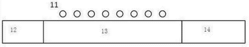
[0032] A specific embodiment of a low-temperature polysilicon thin film manufacturing method described in the present invention is given below, a low-temperature polysilicon thin film manufacturing method, on the basis of maintaining the solid phase crystallization ambient temperature at 550-700 degrees Celsius, one or more Light source with photon energy in the range of 2.5-5.0eV. The low-temperature polysilicon film manufacturing method comprises the following three steps:

[0033] In the first step, the local polysilicon forms crystal nuclei with a diameter larger than the critical dimension under the action of thermal fluctuations;

[0034] In the second step, the crystal nuclei grow to form crystal grains;

[0035] In the third step, the adjacent grain boundaries are closed to complete the transition from amorphous silicon to polysilicon, and the internal defect states of the polysilicon are gradually repaired to form a polysilicon film.

[0036] In this embodiment, in ...

Embodiment 2

[0039] The light source is only added in the first step, the photon energy is 2.0eV, the irradiation time is 8 minutes, and the number of light sources is two ultraviolet light sources. As other convertible implementations, the energy of the photons added in the first step can also be selected to be 3.0eV, the heating time is 10 minutes, and the number of light sources is three; or a 4.0eV light source is added, and the heating time is 15 minutes. The number is 1. The function of adding a light source in the first step is to assist the formation of crystal nuclei and increase the temperature of the amorphous silicon film. The photon energy is selected from 2.0-4.0eV, and amorphous silicon has good absorption in this band. The heating time is about 5-15 minutes.

Embodiment 3

[0041] The light source is only added in the second step, the photon energy is 4.0eV, the irradiation time is 120 minutes, and the number of light sources is three ultraviolet light sources. As other convertible implementations, the energy of the photons added in the second step can also be selected as 4.5eV, the heating time is 20 minutes, and the number of light sources is two; or a 4.2eV light source is added, and the heating time is 60 minutes. The number is one. The role of adding light source in the second step is to increase the grain growth rate and inhibit the formation of new crystal nuclei in the amorphous silicon region. The photon energy range is 4.0-4.5eV. In this band, only the crystal grains will have strong absorption. , the absorption of amorphous silicon is not strong. Therefore, the growing crystal grains will be heated to increase their growth rate; on the other hand, amorphous silicon will not be heated, so that too many crystal nuclei will not be formed...


PUM


Abstract

The invention provides a manufacturing method of a low-temperature polysilicon thin film. On a basis that a solid-phase crystallization environmental temperature is maintained at 550-700 DEG C, one or more light sources with photon energy ranges of 2.5-5.0eV are added. According to the invention, under a relatively low temperature, the crystallization rate of the polysilicon thin film is improved, and the defect state density is reduced, such that the low-temperature polysilicon thin film can be manufactured. The polysilicon thin film provided by the invention has relatively high crystallization rate. A thin-film transistor back-plate produced by using the polysilicon thin film has a mobility enough for driving AMOLED, and relatively high homogeneity. Therefore, a semiconductor thin film material for producing high-quality AMOLED panels can be ensured.

Description

technical field [0001] The invention relates to a method for manufacturing a low-temperature polysilicon film, in particular to a solid-phase crystallization method for reducing the defect state density of a polysilicon film. Background technique [0002] AMOLED (Active Matrix Organic Light Emitting Diode, Active Matrix Organic Light Emitting Diode) is an active light emitting device. Compared with the current mainstream flat panel display technology TFT-LCD (Thin Film Transistor-Liquid Crystal Display, Thin Film Transistor Liquid Crystal Display), OLED (Organic Light Emitting Diode, Organic Light Emitting Diode) has high contrast, wide viewing angle, low power consumption, volume Thinner and other advantages, it is expected to become the next-generation flat panel display technology after LCD, and it is one of the most concerned technologies in flat panel display technology at present. [0003] OLED is driven by current, so the driving circuit of each pixel must ensure a l...

Claims


Application Information

Patent Timeline
IPC IPC(8): C30B1/02C30B28/02
Inventor 林立邱勇黄秀颀施露张洁
Owner CHENGDU VISTAR OPTEOLECTRONICS CO LTD
Why Eureka
Try Eureka