Bigrid power MOSFET (Metal-Oxide-Semiconductor Field Effect Transistor) device

A device and power technology, applied in the field of low-power MOS control semiconductor power devices, can solve the problems of reduced on-resistance and low concentration in the drift region, so as to reduce the on-resistance and power consumption, increase the current flow area, and shorten the current The effect of the conduction path

Inactive Publication Date: 2012-10-17
UNIV OF ELECTRONICS SCI & TECH OF CHINA
View PDF3 Cites 17 Cited by
  • Summary
  • Abstract
  • Description
  • Claims
  • Application Information

AI Technical Summary

Problems solved by technology

However, the current passing through the groove gate channel has to go through a long drift region, and the concentration of this drift region is low, which limits the further reduction of on-resistance

Method used


Image

  • Bigrid power MOSFET (Metal-Oxide-Semiconductor Field Effect Transistor) device
  • Bigrid power MOSFET (Metal-Oxide-Semiconductor Field Effect Transistor) device
  • Bigrid power MOSFET (Metal-Oxide-Semiconductor Field Effect Transistor) device

Examples


Embodiment 1

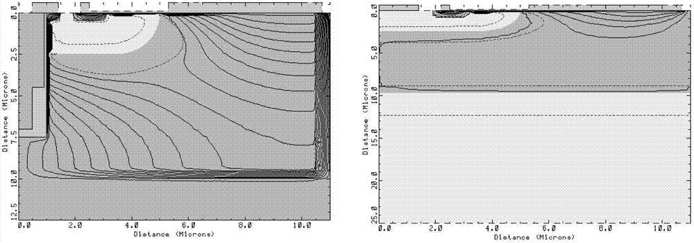
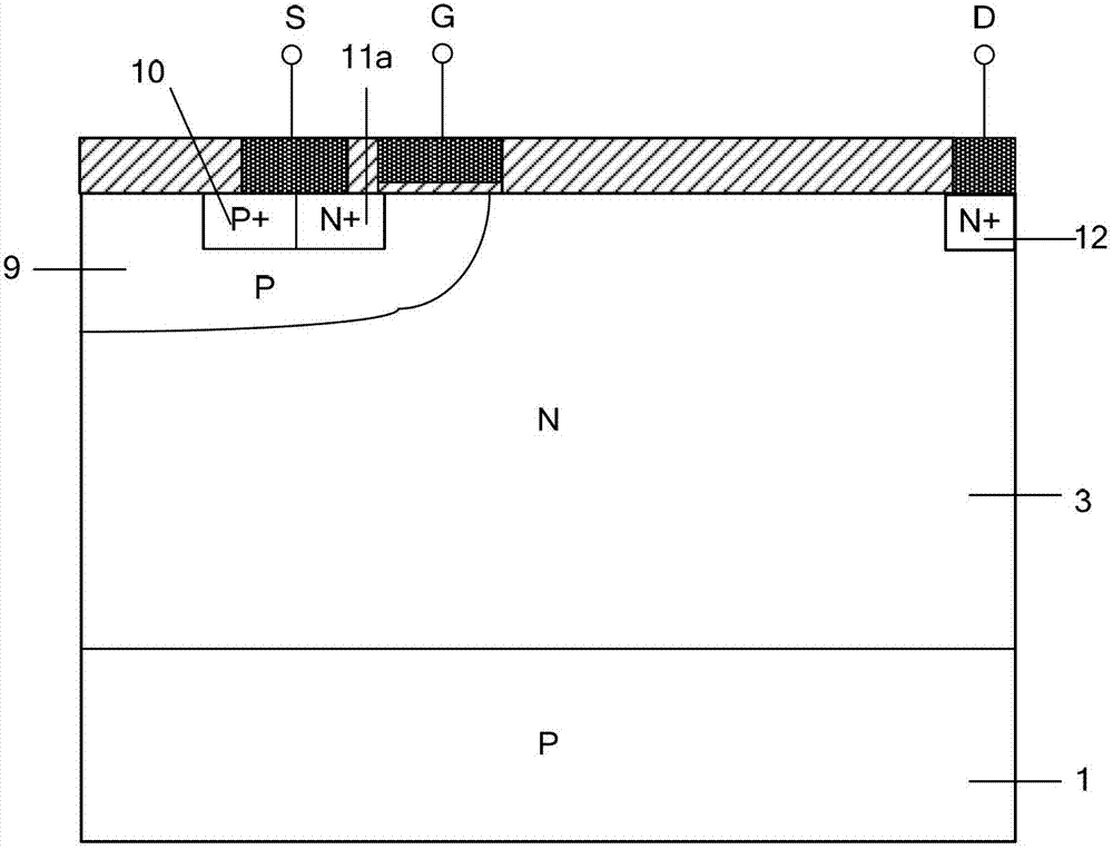
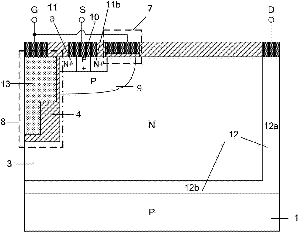
[0028] figure 1 It is a schematic diagram of the cross-sectional structure of a conventional LDMOS device for comparison; figure 2 It is a schematic diagram of the cross-sectional structure of an N-channel double-gate MOSFET device proposed by the present invention.

[0029] A dual-gate power MOSFET device such as figure 2 , including a P-type semiconductor substrate 1, an N-type semiconductor active layer 3, a planar gate structure 7, a trench gate structure 8, a source structure and a drain structure, wherein the top of the N-type semiconductor active layer 3 has a P-type semiconductor body area 9. The source structure includes a source metal, an N-type heavily doped semiconductor source contact region 11 and a P-type heavily doped semiconductor body contact region 10, wherein the N-type heavily doped semiconductor source contact region 11 includes N Type first heavily doped semiconductor source contact region 11a and N type second heavily doped semiconductor source co...

Embodiment 2

[0032] image 3 It is a schematic cross-sectional structure diagram of a dual-gate power MOSFET device (N-channel) provided by the present invention (with a uniform thickness of the trench gate dielectric). The difference between the embodiment 2 and the embodiment 1 is that the thickness of the trench gate dielectric 4 in the longitudinal direction is not in a stepped shape with the top thin and the bottom thick, but is made to be uniform in thickness. This is simpler than embodiment 1 in technology.

Embodiment 3

[0034] Figure 4 It is a schematic cross-sectional structure diagram of a dual-gate power MOSFET device (P channel) provided by the present invention (with a uniform thickness of the trench gate dielectric). Such as Figure 4 shown, which is the same as image 3 The only difference is that the semiconductor material conductivity type of the substrate 1, the active layer 3, the source regions 11a, 11b, the drain region 12, the body region 9 and the body contact region 10 of the device in this example and the N-channel double gate The corresponding area of ​​the lateral MOSFET device is reversed. That is to say, the dual-gate MOSFET device with semiconductor buried layer of the present invention can be used to manufacture N-channel MOSFET devices and P-channel MOSFET devices.


PUM


Abstract

The invention discloses a bigrid power MOSFET (Metal-Oxide-Semiconductor Field Effect Transistor) device, belonging to the technical field of semiconductor power devices. According to the invention, on the basis of a common bigrid LDMOS (Laterally Diffused Metal Oxide Semiconductor) device, by means of extending a drain-electrode contact area connected with drain-electrode metal to a place below an active layer to form a longitudinal drain-electrode contact area (12a) and introducing a layer of heavily-doped buried layer namely a transverse drain-electrode contact area (12b) connected with the lower end of the longitudinal drain-electrode contact area (12a) between the active layer and the substrate, a current conduction path is shortened; meanwhile, a bigrid structure is adopted to form a double-current channel, so that the current flow area is enlarged, and on-resistance and power consumption are reduced greatly; and compared with the devices with the same transverse dimensions, the device disclosed by the invention is slightly reduced in withstand voltage.

Description

technical field [0001] The invention belongs to the technical field of semiconductor power devices, and relates to a low-power MOS control semiconductor power device with a double gate structure. Background technique [0002] Power MOSFET (metal oxide semiconductor Field-Effect Transistor) is a multi-subconduction device with high input impedance, easy driving, fast speed, high frequency, positive temperature coefficient of on-resistance, wide safe operating area, and parallel use, etc. advantage. These advantages make it widely used in industrial control, aerospace, communications, automobiles, computers and portable appliances, home appliances, office supplies and other fields, especially in the application of switching power supplies, which has achieved rapid development and greatly improved the efficiency of electronic systems . [0003] Devices with a grooved gate structure have the following advantages: First, the packaging density can be increased, thereby increasin...

Claims


Application Information

Patent Timeline
Patent Type & Authority Applications(China)
IPC IPC(8): H01L29/78H01L29/423
CPCH01L29/42368H01L29/4238H01L29/7825H01L29/7831
Inventor 罗小蓉周坤姚国亮蒋永恒王沛王琦罗尹春蔡金勇范叶范远航王骁玮
Owner UNIV OF ELECTRONICS SCI & TECH OF CHINA
Why Eureka
Try Eureka