
Nanometer impression device and nanometer impression method for high-brightness light-emitting diode (LED) graphics

A nano-imprinting and patterning technology, which is applied in the direction of nanotechnology, nanotechnology, nanotechnology, etc. for information processing, can solve the problems of mold damage, difficulty in large-area demoulding, high cost, etc., and achieve the goal of reducing imprinting defects Effects of production, good conformal contact capability, solution lifetime and cost

Active Publication Date: 2013-01-09
兰红波
View PDF11 Cites 31 Cited by
  • Summary
  • Abstract
  • Description
  • Claims
  • Application Information

AI Technical Summary

Problems solved by technology

Therefore, it is extremely difficult to manufacture large-area, high-aspect-ratio micro-nano structures on the surface of non-flat LED epitaxial wafers or sapphire substrates efficiently, at low cost, and on a large scale by using various existing micro-nano manufacturing methods, which cannot meet the needs of LEDs. Demand for Graphical Industrial Grade Applications
For example, due to the warping, bending, surface wavy shape and sharp protrusions of LED epitaxial wafers, the focal depth ratio of traditional optical lithography cannot meet the requirements of exposure; the use of electron beam lithography to manufacture large-area nanostructures has high costs and low productivity. Difficult to achieve large-scale, large-scale manufacturing
For NPSS, the use of existing contact or proximity lithography equipment cannot meet the requirements of nano-pattern manufacturing accuracy. Although stepper projection lithography (Stepper) can be used to achieve NPSS manufacturing, the Stepper used in the semiconductor industry is in the LED industry. Too expensive, greatly increasing the manufacturing cost of LEDs
LEDs are very sensitive to cost
In addition, some companies currently use second-hand refurbished Stepper, but there are problems in product yield and equipment reliability.
Interference lithography has great advantages in the manufacture of large-area periodic micro-nano structures, but this method has significant shortcomings: small depth of focus, poor selectivity of nano-structure patterns, and harsh requirements for the production environment (compared to LED production process Poor compatibility), especially at present, almost no commercial company provides a mature interference lithography machine (manufacturing of large-scale wafer nanopatterns)
However, the existing nanoimprint process applied to LED patterning still has many deficiencies in terms of mold life, productivity, yield, and reliability. In particular, it still faces some challenging technical problems, such as large-area demoulding difficulties and soft mold deformation. , granular dirt and sharp protruding defects for mold damage, consistency and repeatability of embossed graphics, etc.

Method used


Image

  • Nanometer impression device and nanometer impression method for high-brightness light-emitting diode (LED) graphics
  • Nanometer impression device and nanometer impression method for high-brightness light-emitting diode (LED) graphics
  • Nanometer impression device and nanometer impression method for high-brightness light-emitting diode (LED) graphics

Examples


Embodiment Construction

[0071] The present invention will be further described below in conjunction with the accompanying drawings and embodiments.

[0072] The present invention is an embodiment with the nano-patterned 4-inch sapphire substrate, the substrate 3 is a 4-inch sapphire, the graphic layer 501 of the film-like composite elastic soft mold selects water-soluble polymer polyvinyl alcohol (polyvinyl alcohol, PVA), and the supporting layer 502 uses highly transparent and elastic film-like PET material.

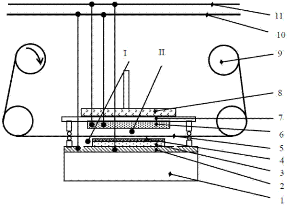
[0073] figure 1It is a schematic structural diagram of the nanoimprinting device used for high-brightness LED patterning in the present invention, which includes: a substrate 1, a vacuum chuck 2, a substrate 3, a UV-curable nanoimprinting resist 4, a mold 5, and a gas Valve plate 6, embossing mechanism 7, ultraviolet light source 8, mold feeding mechanism 9, vacuum pipeline 10, pressure pipeline 11; among them, the substrate 3 coated with UV-curable nanoimprint resist 4 is adsorbed On the va...


PUM


Abstract

The invention discloses a nanometer impression device and a nanometer impression method for high-brightness light-emitting diode (LED) graphics. The nanometer impression device comprises a wafer bearing platform, a vacuum sucking disc, a substrate, a ultraviolet light cured nanometer impression slushing compound and the like. A die is a thin film elastic composite flexible die and comprises a graphical layer and a supporting layer, wherein the graphical layer has the characteristics of water solubility, thin-film structure, elasticity and high transparency, and the die is manufactured by adopting a rolling impression process. The nanometer impression method for achieving high-brightness LED graphics based on the device comprises the steps of (1) pre-processing, (2) impression, (3) curing, (4) demoulding, (5) post-processing and (6) transferring of impression graphics. By means of the nanometer impression device and the nanometer impression method, a large-area, high-aspect-ratio micro-nanometer structure is efficiently manufactured on an unsmooth surface or a curved surface substrate or a fragile substrate with low cost. The nanometer impression device and the nanometer impression method are suitable for large-scale manufacture of optical devices, three-dimensional miniature batteries, micro-electromechanical system (MEMS) devices, photovoltaic devices, anti-reflecting layers, self-cleaning surfaces and the like and are especially suitable for the LED graphics and industrial-grade large-scale production of wafer-level splicing-free micro-optical devices.

Description

technical field [0001] The invention belongs to the technical field of micro-nano manufacturing and optoelectronic device manufacturing, and in particular relates to a nano-imprinting device and method for high-brightness LED patterning. Background technique [0002] LED patterning (sapphire substrate patterning and LED epitaxial wafer patterning) has been considered by academia and industry to be the most effective way to improve light generation efficiency and light extraction efficiency and improve light source quality (control light emission direction and far-field pattern uniformity) Approaches, namely the so-called nano-patterned sapphire substrate (Nano-Patterned Sapphire Substrate, NPSS) and LED epitaxial wafer patterning technology (Photonic Crystal LED, photonic crystal LED; Nanorod LED, nanorod LED; Nanowire LED, nanowire LED) , is currently considered by the industry as one of the most effective technical means to improve light extraction efficiency and realize u...

Claims


Application Information

Patent Timeline
Patent Type & Authority Applications(China)
IPC IPC(8): G03F7/00B82Y10/00
CPCG03F7/0002G03F7/20G03F7/00H01L33/0095H01L2933/0083B82Y40/00B82Y10/00
Inventor 兰红波
Owner 兰红波
Learn More