Preparation method of three-dimensional self-supporting micro-nano functional structure based on thin film material

A technology of functional structure and support structure, which is applied in the field of preparation of three-dimensional self-supporting micro-nano functional structures based on thin film materials, can solve the problem that high aspect ratio pattern metallization or functionalization cannot be realized, pattern resolution depends on exposure spot, Inability to prepare metal materials, etc., to achieve high flexibility and operability, unique functions, and the effect of expanding the scope of preparation

Active Publication Date: 2013-04-17
INST OF PHYSICS - CHINESE ACAD OF SCI
View PDF6 Cites 14 Cited by
  • Summary
  • Abstract
  • Description
  • Claims
  • Application Information

AI Technical Summary

Problems solved by technology

However, the existing three-dimensional micro-nano device preparation methods have various defects: the pattern size of the three-dimensional structure prepared by two-photon interference exposure, laser ablation, laser interference exposure and other processes is greatly affected by the size of the laser spot, and the prepared The minimum size of three-dimensional graphics is on the order of microns; the graphic resolution of the grayscale exposure process depends on the size of the exposure spot. For electron beam grayscale exposure, the resolution can reach nanometers, but the grayscale exposure prepared The three-dimensional structure is relatively simple, and grayscale exposure is powerless for the preparation of self-supporting three-dimensional nanostructures, and it is also impossible to achieve metallization or functionalization of high-aspect ratio graphics; focused electron beam / ion beam etching, assisted deposition Self-supporting three-dimensional micro-nano structures can be prepared, but not only it takes a lot of time, but also cannot prepare high-purity metal materials

Method used


Image

  • Preparation method of three-dimensional self-supporting micro-nano functional structure based on thin film material
  • Preparation method of three-dimensional self-supporting micro-nano functional structure based on thin film material
  • Preparation method of three-dimensional self-supporting micro-nano functional structure based on thin film material

Examples


Embodiment 1

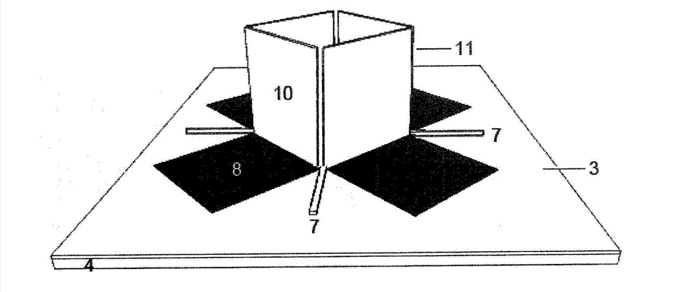
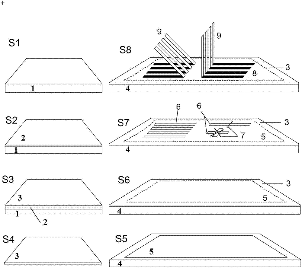
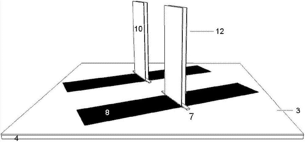
[0045] Using "a method for preparing a three-dimensional self-supporting micro-nano functional structure array" to prepare a three-dimensional metal metamaterial structure array (taking a single-layer gold film as an example), includes the following steps:

[0046] (1) Silicon substrate cleaning

[0047] The silicon substrate was cleaned with acetone, ethanol and deionized water in sequence, then blown dry with nitrogen, baked on a hot plate at 180 degrees Celsius for 10 minutes, and allowed to cool naturally.

[0048] (2) Application of transition layer 2

[0049] Coat one deck electron beam photoresist PMMA (495,5%) on the clean and smooth Si substrate that step (1) has processed (1300 rev / mins, 180 degrees centigrade baking 1 minute after spin-coating, can repeat spin-coating ).

[0050] (3) Preparation of metallic gold nanofilm 3

[0051] On the substrate 1 coated with electron beam photoresist PMMA, a gold thin film layer 3 with a thickness of 100 nanometers is deposit...


PUM


Abstract

The present invention relates to a preparation method of a three-dimensional self-supporting micro-nano functional structure based on a thin film material, comprising the steps of: preparing a transition layer on a clean smooth substrate; preparing nano thin film and peeling nano thin film from a smooth substrate; preparing a supporting substrate with a pore structure; transferring the nano thin film to the supporting substrate with the pore structure; preparing a micro-nano graph on the nano thin film; and inducing the micro-nano graph on the nano thin film by ion beam irradiation to deform and form a finished product with the three-dimensional self-supporting micro-nano structure. The present invention is a novel method for preparing the self-supporting three-dimensional micro-nano functional structure based on the combination of the preparation of micro-nano structure on the nano thin film and ion beam irradiation-induced three-dimensional deformation, and has the characteristics of flexible technology, high efficiency, good controllability, low cost and large-scale preparation. The prepared micro-nano graph is designable in structure, morphology, size, and cycle, is various in material types, and has the characteristics of novel functions and physical properties.

Description

technical field [0001] The invention relates to the technical field of three-dimensional micro-nano devices, and is a method for manufacturing three-dimensional self-supporting micro-nano functional structures and arrays, in particular to a method based on the growth of nano-film materials, the processing of micro-nano patterns on supported nano-films, and ion beam irradiation The technique of deforming and manipulating micro-nano patterns in the plane of the supported nano-film to prepare three-dimensional micro-nano functional structures and devices that are not located in the plane of the supporting substrate. Background technique [0002] With the development of microelectronics technology, the difficulty of device miniaturization is gradually increasing. The structure of three-dimensional devices has undoubtedly become an important way to increase the integration density of devices. Finding a method for fabricating three-dimensionally controllable spatial nanostructures...

Claims


Application Information

Patent Timeline
Patent Type & Authority Applications(China)
IPC IPC(8): B81C1/00
Inventor 李无瑕崔阿娟刘哲顾长志
Owner INST OF PHYSICS - CHINESE ACAD OF SCI
Why Eureka
Try Eureka