Organic solar battery and preparation method of organic solar battery
A solar cell and organic technology, applied in circuits, photovoltaic power generation, electrical components, etc., can solve the problems of complex preparation process, large current loss, and high manufacturing cost, and achieve the effects of broadening the absorption spectrum, low cost, and simple manufacturing process.
- Summary
- Abstract
- Description
- Claims
- Application Information
AI Technical Summary
Problems solved by technology
Method used
Image
Examples
preparation example Construction
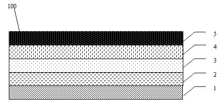
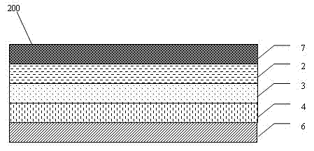
[0038] A method for preparing an organic solar cell, the method comprising the steps of:
[0039] 1) Clean the transparent anode. After etching the electrode pattern, use pure water, absolute ethanol, acetone and isopropanol to sonicate for 10 minutes each in sequence; after drying, treat with UV / ozone (power 70W) for 10-20 minutes.
[0040] 2) Depositing a hole transport layer on the surface of the transparent anode treated above. PEDOT:PSS layer can be prepared by any one of spin coating, spray coating, micro gravure coating and slit coating; MoO 3 , V 2 o 5 Or the NiO layer can be prepared by any one of magnetron sputtering, ion sputtering, vacuum evaporation and atomic layer deposition.
[0041] 3) Under the protection of nitrogen, the organic active liquid doped with quantum dot nanoparticles is prepared on the surface of the hole transport layer by any coating method such as spin coating, spray coating, microgravure coating, and slit coating, and heated or Vacuum dr...
Embodiment 1
[0047] 1) Etch the anode pattern with 2cm×3cm PET / ITO (Zhuhai Kaiwei Electronic Components Co., Ltd., square resistance 32Ω / □, transmittance 83%), wash with detergent, and then use pure water and absolute ethanol in sequence , acetone and isopropanol ultrasonic vibration for 10 minutes, after drying, UV / ozone (power 70W) treatment for 10 minutes before use;
[0048] 2) Spin-coat a PEDOT:PSS hole transport layer with a thickness of 42nm on the surface of the transparent anode in air, and dry at 110°C for 10 minutes;
[0049] 3) Under the protection of nitrogen, the organic active layer P3HT (absorbing Peak 535nm): PC 61 BM (P3HT:PC 61 BM:CdSeS=50:50:5, weight ratio), annealed at 130°C for 10min;
[0050] 4) Deposit a LiF electron transport layer with a thickness of 0.7 nm on the surface of the organic active layer by vacuum evaporation;
[0051] 5) With the help of a square mask, vacuum-evaporate Al with a thickness of 120 nm on the surface of the electron transport layer a...
Embodiment 2
[0054] 1) After etching the anode pattern on 2cm×3cm FTO conductive glass (NSG Japan, square resistance 5.1Ω / □, transmittance 86%), wash it with detergent, and then use pure water, absolute ethanol, acetone and isocyanate in sequence. Ultrasonic oscillation with propanol for 10 minutes, after drying, UV / ozone (power 70W) treatment for 20 minutes before use;
[0055] 2) In air, MoO with a thickness of 10 nm was magnetron sputtered on the surface of the above transparent anode 3 hole transport layer;
[0056] 3) Under the protection of nitrogen, in the hole transport layer MoO 3 The organic active layer PBDTTT-C-T (absorption peaks 631nm and 692nm) containing GaAs quantum dot nanoparticles with a particle size of 9.8nm (emission peak 692nm, peak width 26nm) with a thickness of 110nm sprayed on the surface: PC 71 BM (PBDTTT-C-T:PC 71 BM: GaAs=40:60:10, weight ratio), vacuum dried;
[0057] 4) A ZnO electron transport layer with a thickness of 8nm is deposited on the surface o...
PUM
| Property | Measurement | Unit |
|---|---|---|
| Particle size | aaaaa | aaaaa |
| Particle size | aaaaa | aaaaa |
| Thickness | aaaaa | aaaaa |
Abstract
Description
Claims
Application Information

