Bicyclo-iridium complex, preparation method of complex, organic light emitting diode (OLED) and preparation method of OLED

A technology of electroluminescent devices and iridium complexes, which is applied in the fields of organic semiconductor devices, electric solid devices, semiconductor/solid device manufacturing, etc., can solve problems such as backward research progress, difficulties, and small energy level difference of compounds, and achieve external quantum efficiency High, stable luminous performance, high saturation of red light emission

Inactive Publication Date: 2013-05-22
HEFEI BOE OPTOELECTRONICS TECH +1
View PDF3 Cites 5 Cited by
  • Summary
  • Abstract
  • Description
  • Claims
  • Application Information

AI Technical Summary

Problems solved by technology

[0004] To achieve application and industrialization of organic electroluminescent devices, one of the key factors is to improve luminous efficiency and brightness. The improvement of efficiency and brightness depends not only on the performance of the designed device, but also on the realization of full-color display and lighting. For application purposes, red light is indispensable among the three primary colors. Compared with high-performance green light-emitting devices, the research progress of red light-emitting devices in the prior art lags behind. The reasons for this situation include: (1) corresponding to red The energy level difference of the light-emitting compound is small, which adds some difficulties to the design of the ligand of the red light material; (2) In the red light material system, there is a strong π-π bond interaction, or has a strong charge transfer performance , will aggravate the aggregation of molecules and easily lead to quenching phenomenon

Method used


Image

  • Bicyclo-iridium complex, preparation method of complex, organic light emitting diode (OLED) and preparation method of OLED
  • Bicyclo-iridium complex, preparation method of complex, organic light emitting diode (OLED) and preparation method of OLED
  • Bicyclo-iridium complex, preparation method of complex, organic light emitting diode (OLED) and preparation method of OLED

Examples


preparation example Construction

[0079] The embodiment of the present invention also provides a preparation method of the above-mentioned bicyclic iridium complex, and the preparation method specifically includes the following steps:

[0080] Step (1), dissolving phosphorus pentoxide in m-cresol, then adding 1-naphthalene-1-yl-ethanone and anthranilaldehyde derivatives for dehydration reaction to obtain 2-naphthalene- 1-yl-quinoline derivatives;

[0081]

[0082] Step (2), the IrCl 3 ﹒ 3H 2 O is dissolved in water, adding the 2-naphth-1-yl-quinoline derivative and the first organic solvent, in N 2 Stir in the dark in the environment to obtain the dichloro bridge compound of iridium shown in the following structural formula;

[0083]

[0084] In step (3), the dichloro bridge compound of iridium is dissolved in a second organic solvent, and stirred with an auxiliary ligand under the action of a base to obtain the bicyclic iridium complex.

[0085] Wherein, in step (1), preferably, the dosage ratio of...

Embodiment 1

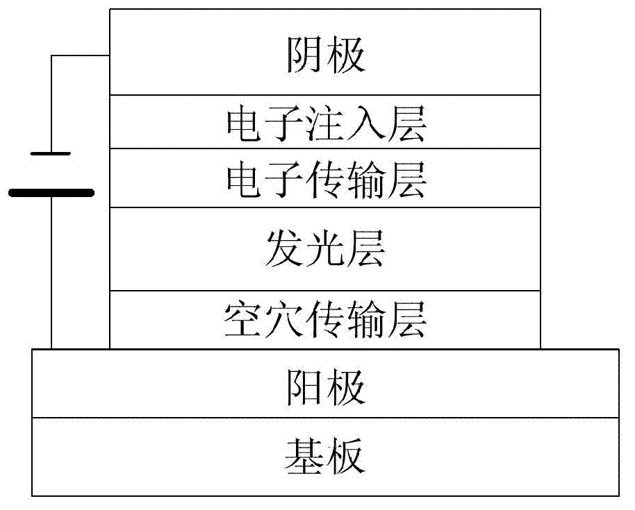
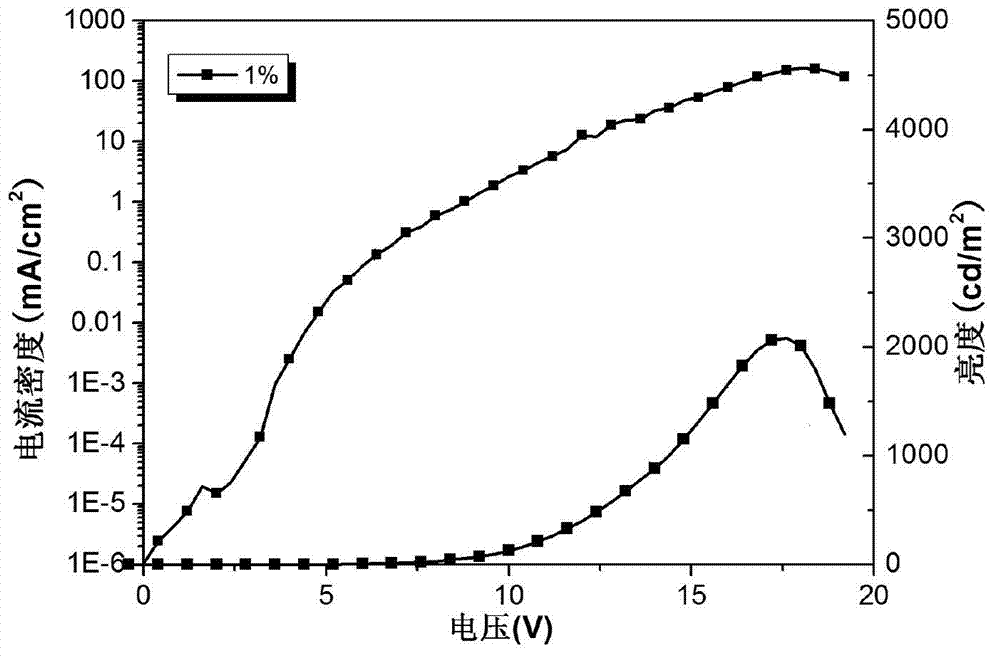
[0109] In this embodiment, the structure of the organic electroluminescent device is: the anode is made of indium tin oxide (ITO); the hole transport layer is made of PEDOT / PSS (3,4-ethylenedioxythiophene polymer doped polystyrene sulfonic acid ), the thickness is 40nm; the thickness of the light-emitting layer is 70nm; the electron transport layer is TPBI (1,3,5-tris(1-phenyl-1H-benzimidazol-2-yl)benzene), the thickness is 30nm; the electron injection The layer uses cesium fluoride (CsF) with a thickness of 1.5nm; the cathode uses aluminum (Al) with a thickness of 120nm. Among them, in the light-emitting layer, PVK, PBD and (NPQ) 2 The mass ratio of Ir(pic) is 69:30:1.

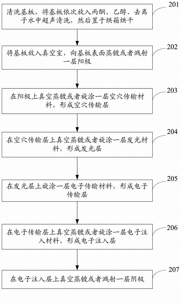
[0110] The preparation method of the organic electroluminescence device of the present embodiment comprises the following steps:

[0111] A: After cleaning the indium tin oxide (ITO) conductive glass substrate ultrasonically in acetone, detergent, deionized water and isopropanol liquid, put it in an oven fo...

Embodiment 2

[0118] In this embodiment, the structure of the organic electroluminescent device is as follows: the anode is made of ITO; the hole transport layer is made of PEDOT / PSS with a thickness of 40nm; the thickness of the light-emitting layer is 70nm; CsF is used with a thickness of 1.5nm; the cathode is made of Al with a thickness of 120nm. Among them, in the light-emitting layer, PVK, PBD and (NPQ) 2 The mass ratio of Ir(pic) is 69:29:2.

[0119] The preparation method of the organic electroluminescence device of the present embodiment comprises the following steps:

[0120] A: After ultrasonically cleaning the indium tin oxide (ITO) conductive glass substrate in acetone, detergent, deionized water and isopropanol liquid, put it in an oven for drying, and then perform oxygen plasma treatment on the cleaned substrate to improve the ITO The work function can further remove the residual organic dirt on the surface of the ITO substrate and improve the contact angle of the substrate ...


PUM

PropertyMeasurementUnit
thicknessaaaaaaaaaa
thicknessaaaaaaaaaa
thicknessaaaaaaaaaa

Abstract

The invention provides a bicyclo-iridium complex, a preparation method of the complex, an organic light emitting diode (OLED) and a preparation method of the OLED, which belong to the field of organic electroluminescence. A light emitting layer of the OLED comprises the bicyclo-iridium complex with the following structure shown in the specification, wherein substituent groups R1 and R2 can be same or different. The OLED provided by the embodiment of the invention has the advantages of high external quantum efficiency, high red luminescence saturation degree and stable luminescence property.

Description

technical field [0001] The invention relates to the field of organic electroluminescence, in particular to a bicyclic iridium complex and a preparation method, an organic electroluminescence device and a preparation method. Background technique [0002] In the prior art, the practical displays mainly include cathode ray tube (CRT), liquid crystal display (LCD), vacuum fluorescent device (VFD), plasma display (PDP), organic electroluminescent device (OLED), field emission display ( FED) and electroluminescent display (ELD), etc. [0003] As a new type of flat-panel display, compared with LCD, OLED has the advantages of thinness, lightness, wide viewing angle, active light emission, continuously adjustable light color, low cost, fast response speed, low energy consumption, low driving voltage, wide operating temperature range, and excellent production process. Due to the advantages of simplicity, high luminous efficiency and flexible display, OLED has attracted great attentio...

Claims


Application Information

Patent Timeline
Patent Type & Authority Applications(China)
IPC IPC(8): C07F15/00C09K11/06H01L51/54
CPCC09K2211/1007C07F15/0033C09K2211/185C09K2211/1029C07F15/00C09K2211/1011C09K11/06C09K2211/145C09K2211/1475C09K11/02C09K2211/1466H10K85/146H10K85/1135H10K85/6565H10K85/342H10K85/6572H10K50/11H10K2101/90C09K2211/1048
Inventor 郭远辉王辉叶欣秦锋
Owner HEFEI BOE OPTOELECTRONICS TECH
Why Eureka
Try Eureka