
A kind of preparation method of silicon carbide microstructure

A technology of silicon carbide and microstructure, applied in the direction of microstructure technology, microstructure devices, manufacturing microstructure devices, etc., can solve the problems of complex process flow and low material etching rate, and achieve the effect of good corrosion selectivity

Active Publication Date: 2016-06-08
XI AN JIAOTONG UNIV
View PDF4 Cites 0 Cited by
  • Summary
  • Abstract
  • Description
  • Claims
  • Application Information

AI Technical Summary

Problems solved by technology

However, the process flow of this method is complicated, and the etching rate of the material is not high, the typical rate is 0.5 μm / min

Method used


Image

  • A kind of preparation method of silicon carbide microstructure
  • A kind of preparation method of silicon carbide microstructure
  • A kind of preparation method of silicon carbide microstructure

Examples


preparation example Construction

[0025] The preparation method of the silicon carbide microstructure of the present invention is to use femtosecond laser irradiation in a gas environment to induce a silicon carbide-based refractive index change structure on a silicon carbide substrate by means of scanning, and then pass hydrofluoric acid and The mixed solution of nitric acid is etched to remove the area of ​​refractive index change, thereby preparing the silicon carbide microstructure. The present invention is applicable to silicon carbide crystals of various types and crystal orientations, and the commonly used 6H-SiC crystals with hexagonal close packing and crystal orientation are preferred. The method specifically follows the steps below:

[0026] (1) Select a silicon carbide wafer as the substrate, and ultrasonically clean it in acetone, alcohol, and deionized water in sequence; the crystal type of the silicon carbide substrate is any crystal orientation, such as or . Alternatively, the crystal type o...

Embodiment 1

[0035] (1) Select a 6H-SiC crystal with a crystal orientation of , a thickness of 300 μm, and double-sided polishing as the substrate, and ultrasonically clean it in acetone, alcohol, and deionized water in sequence, and the cleaning time is 20 minutes;

[0036] (2) In the air environment, using femtosecond laser irradiation, the refractive index change area is induced on the silicon carbide substrate by scanning; in this step, the depth, width and aspect ratio of the refractive index change structure can be By changing the laser irradiation conditions, such as laser power, scanning rate and focusing conditions, etc., flexible control can be achieved; the laser-induced refractive index change depth can reach 300 μm;

[0037] (3) The silicon carbide substrate irradiated by femtosecond laser is chemically wet-etched in a mixed solution of hydrofluoric acid and nitric acid to remove the area where the refractive index changes; in this step, the mass percentages are 40% Mix with 6...

Embodiment 2

[0040] The original material used in this embodiment: double-sided polished 6H-SiC, crystal orientation , and a thickness of 300 μm. The specific steps of preparation are as follows:

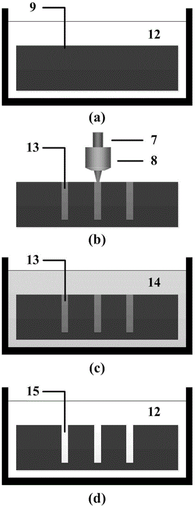
[0041] (1) Use acetone, alcohol and deionized water to clean silicon carbide in an ultrasonic cleaner in sequence, each cleaning time is 20mins, such as figure 2 as shown in (a);

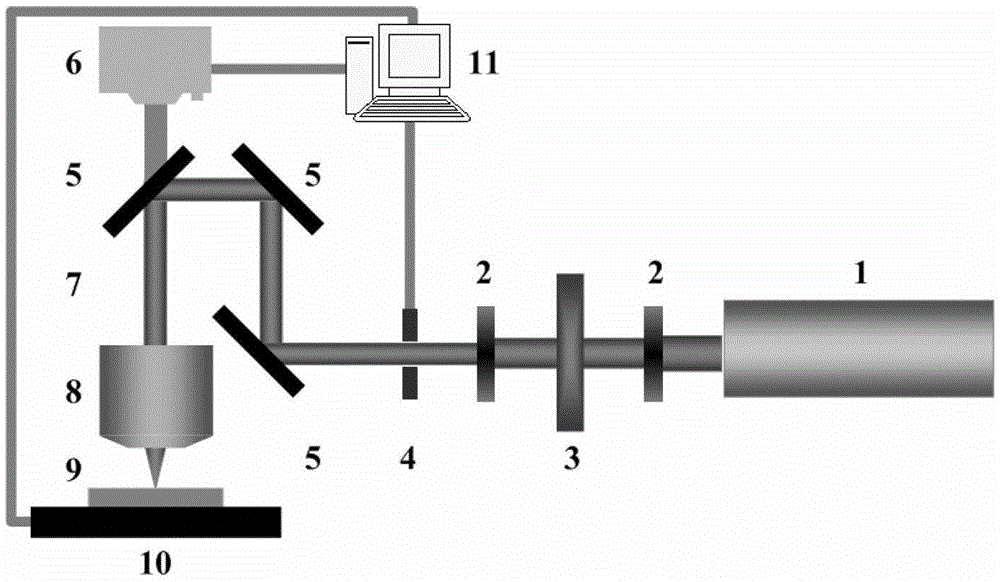
[0042] (2) Fix the cleaned sample on the three-dimensional mobile platform 10, select an optical microscope 8 with a magnification of 5×, and a numerical aperture of 0.30, focus the femtosecond laser beam 7 on the silicon carbide substrate 9, and perform the test on the computer 11 Set the scan rate as 5 μm / s above, and set the laser power as 40 mW by adjusting the variable attenuation sheet. By scanning, a refractive index change microstructure 13 is induced on the silicon carbide substrate, such as figure 2 As shown in (b), its depth is about 280 μm, its half-maximum width is about 10 μm, and its aspect ratio i...


PUM

PropertyMeasurementUnit
thicknessaaaaaaaaaa
depthaaaaaaaaaa
depthaaaaaaaaaa

Abstract

The invention discloses a method for preparing silicon carbide micro-structures. The method includes the steps that in a gaseous environment, femtosecond laser irradiation is utilized, a refractive index change region is generated on a silicon carbide substrate in an induced mode in a scanning mode, the refractive index change region is corroded and removed by mixed liquor of hydrofluoric acid and nitric acid, and then the silicon carbide micro-structures are prepared. The method is simple in technological process, and distribution of the micro-structures does not need to be defined by a mask plate. Compared with a current frequently-used wet etching method and a current frequently-used dry etching method, the method is better in corrosion selectivity, and an etching region is totally determined by a laser irradiation region. By the utilization of the method, a slot which is high in aspect ratio and free of being polluted by impurity elements can be prepared on the silicon carbide substrate by regulating and controlling laser irradiation parameters. The method can be applied to the field of semiconductor devices and a micro mechanical electronic system.

Description

technical field [0001] The invention belongs to the technical field of semiconductor devices and micromechanical electronic systems, and relates to a silicon carbide microstructure, in particular to a method for preparing a silicon carbide microstructure by combining femtosecond laser irradiation and chemical wet etching. Background technique [0002] Silicon carbide is a wide bandgap semiconductor with high thermal conductivity, high breakdown electric field strength and high maximum current density. In the field of semiconductor devices and micromechanical electronic systems, under extreme conditions (high temperature, high pressure, high power, high frequency) etc.), it can be used as a substitute for silicon. At present, people mainly use dry etching to prepare silicon carbide-based microstructures, such as high aspect ratio slots, which are used in isolation slots in high-power semiconductor components, micro-mechanical electronic systems in extreme environments, carbon...

Claims


Application Information

Patent Timeline
Patent Type & Authority Patents(China)
IPC IPC(8): H01L21/268H01L21/306B81C1/00
Inventor 司金海马云灿陈涛屈文成陈烽侯洵
Owner XI AN JIAOTONG UNIV
Learn More