
Preparation method of silicon and silicon doped nanosheet

A technology of nanosheets and doping elements, which is applied in the field of preparation of silicon and its doped nanosheets, can solve the problems of limiting the practical application of silicon nanosheets, impure products, complex processes, etc., and achieve no harmful substances and low cost , the effect of simple process

Inactive Publication Date: 2014-01-22
DALIAN UNIV OF TECH
View PDF4 Cites 6 Cited by
  • Summary
  • Abstract
  • Description
  • Claims
  • Application Information

AI Technical Summary

Problems solved by technology

However, the above-mentioned preparation methods of silicon nanosheets inevitably have problems such as complicated process, impure products, and high cost. The most fatal shortcoming is that the yield is extremely low, which seriously limits the practical application of silicon nanosheets.

Method used


Image

  • Preparation method of silicon and silicon doped nanosheet
  • Preparation method of silicon and silicon doped nanosheet
  • Preparation method of silicon and silicon doped nanosheet

Examples


Embodiment 1

[0022] The high-purity silicon block is used as the anode, and the tungsten rod is used as the cathode, and the distance between the two electrodes is adjusted to 30mm. Vacuum the reaction chamber to about 10 -2 Pa, filled with argon and hydrogen at a ratio of 2:1 to reach 2×10 4 Pa and 1×10 4 Pa. Turn on the cooling water system, turn on the power and start the arc, adjust the current and the distance between the two electrodes and stabilize the arc, evaporate the bulk target, form atomic clusters and gather them into nanosheets and deposit them on the wall of the reaction chamber, and collect the powder through passivation process.

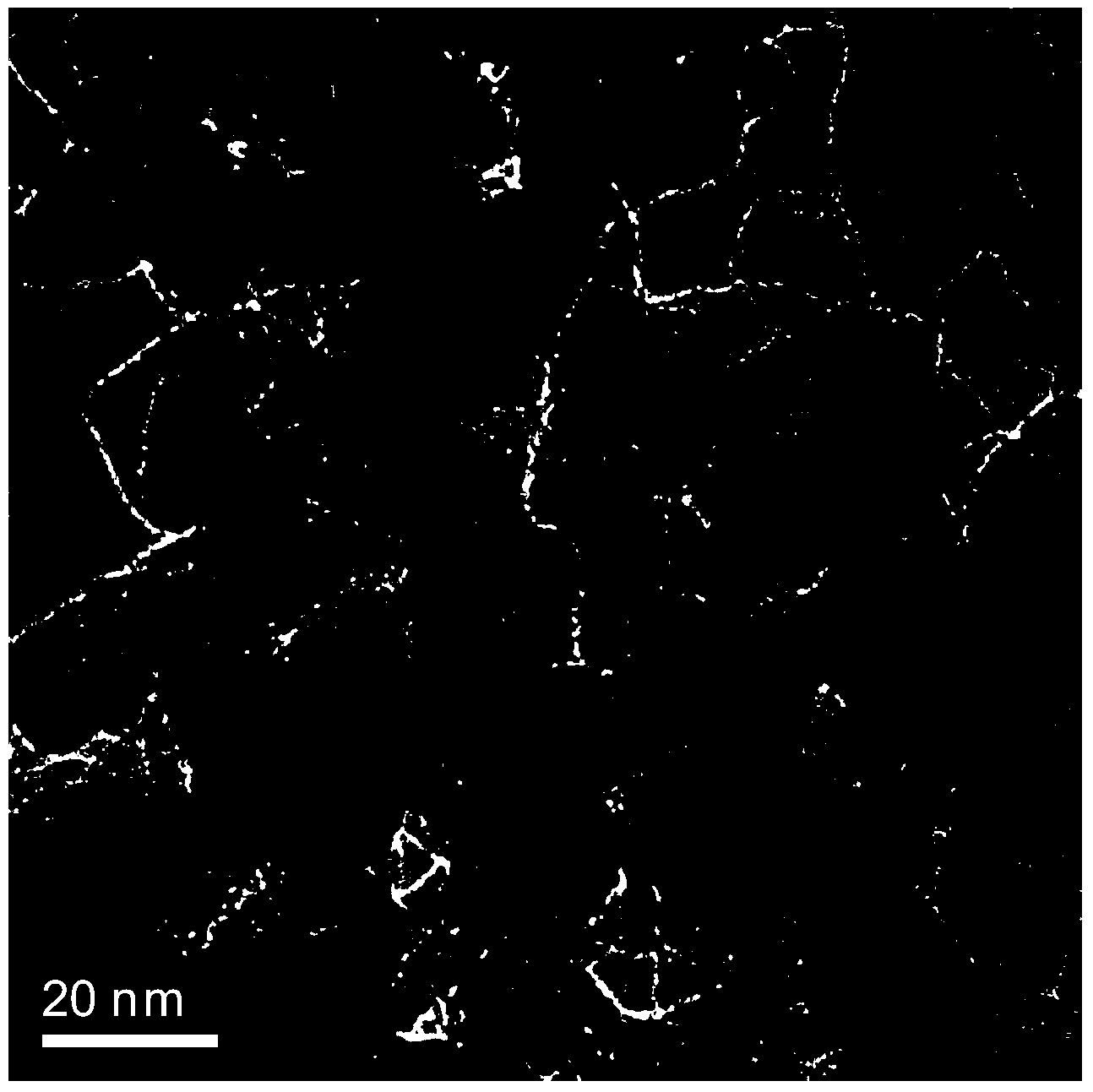
[0023] The TEM image of silicon nanosheets obtained in Example 1 is as follows figure 1 Shown, appear as nanosheets.

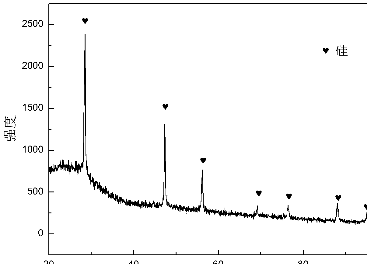
[0024] The obtained silicon nanosheet XRD pattern of embodiment 1 is as follows figure 2 As shown, it is shown as single-phase silicon.

[0025] The silicon nanosheets obtained in Example 1 have a thickness of about 1.5 n...

Embodiment 2

[0027] The high-purity silicon block is used as the anode, and the tungsten rod is used as the cathode, and the distance between the two electrodes is adjusted to 30mm. Vacuum the reaction chamber to about 10 -2 Pa, filled with helium and hydrogen at a ratio of 2:1 to reach 2×10 4 Pa and 1×10 4 Pa. Turn on the cooling water system, turn on the power and start the arc, adjust the current and the distance between the two electrodes and stabilize the arc, evaporate the bulk target, form atomic clusters and gather them into nanosheets and deposit them on the wall of the reaction chamber, and collect the powder through passivation process. Compared with the silicon nanosheets prepared in Example 1, the silicon nanosheets prepared in Example 2 are narrower and have a ribbon-like morphology.

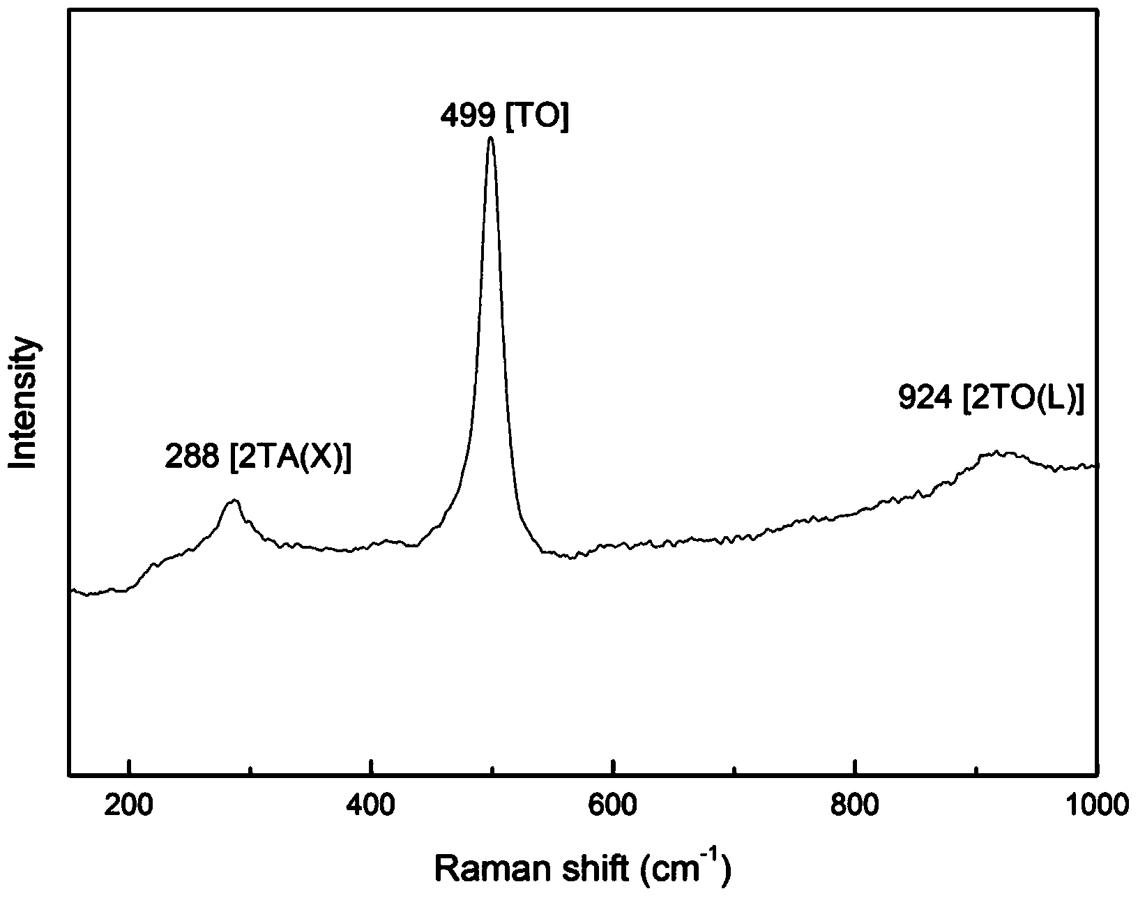
[0028] The obtained silicon nanosheet Raman collection of illustrative plates of embodiment 2 is as image 3 , showing the second-order vibration characteristic peaks of the two-dimensional...

Embodiment 3

[0030] Mix and grind the silicon nanosheets prepared in Example 1, conductive agent and sodium carboxymethyl cellulose with a mass ratio of 45:45:10, add an appropriate amount of deionized water dropwise, and stir to obtain a viscous slurry, which is coated on the pre- On the pressed copper foil, dry in vacuum at 120°C for 10h. Then transfer the electrode sheet to a glove box filled with argon (Ar2 <0.1ppm), the lithium sheet is used as the counter electrode, the electrolyte is 1M LiTFSI, the separator is Ceglard2400 microporous polypropylene membrane, and the CR2025 button half-cell is assembled. CHI660D-1 electrochemical workstation (Shanghai Chenhua Instrument Co., Ltd.) was used to conduct cyclic voltammetry test with a scanning speed of 0.0001V / S and a voltage range of 0.01-2.5V. Using Land CT2001A (Wuhan Landian Electronics Co., Ltd.) for cycle performance test, the voltage range is 0.01-1.2V.

[0031] The lithium-ion battery cycle performance curve that embodiment 3 ga...


PUM

PropertyMeasurementUnit
Thicknessaaaaaaaaaa

Abstract

The invention discloses a preparation method of silicon and a silicon doped silicon doped nanosheet. The preparation method is characterized by comprising the steps of using bulk silicon or bulk silicon doped with elements as an anode and taking a tungsten rod or a molybdenum rod as a cathode, and regulating the distance between the two electrodes to be 10-30mm; vacuumizing a reaction chamber, and filling hydrogen and inert gas according to a certain proportion; connecting automatic control direct-current arc metal nano powder production equipment to a cooling water system, conducing power supply and arcing, and regulating current and the distance between the two electrodes to obtain stable arc; under a hydrogen plasma heat source, evaporating the anode to be in gaseous silicon atom state, thus forming an atom cluster and coagulating nano powder, wherein the atom cluster and the nano powder are deposited on the inner wall of the water-cooled reaction chamber or are delivered into a trapping chamber along a circulating airflow; after completely depositing the nano powder, carrying out passivation, then collecting the powder body, and implementing primary sieving, wherein the silicon nanosheet is 3-500nm in size and 1-5nm in thickness. According to the method, the process is simple, the cost is low, harmful substance does not exist, the yield is high, output is great, and industrial production can be realized.

Description

technical field [0001] The invention belongs to the technical field of nanomaterial preparation, and relates to a method for preparing silicon and its doped nanosheets. Background technique [0002] Materials with two-dimensional nanostructures have attracted more and more attention in recent years. Compared with zero-dimensional and one-dimensional nanomaterials, two-dimensional nanomaterials have more active sites and present more effective surfaces, making two-dimensional nanomaterials show good application prospects in energy, environment, microelectronics and other fields . [0003] In 2004, Geim and Novosselov of the University of Manchester successfully prepared single-layer graphite, namely graphene. Graphene has many unique and excellent properties: such as very high Young's modulus, thermal conductivity, carrier mobility, and specific surface area. It also has phenomena such as fractional quantum Hall effect, quantum Hall ferromagnetism and exciton band gap. It...

Claims


Application Information

Patent Timeline
IPC IPC(8): C01B33/021B82Y30/00B82Y40/00
Inventor 董星龙薛方红于秀红余洁意黄昊于洪涛全燮
Owner DALIAN UNIV OF TECH
Learn More