Inversed organic thin-film solar cell and manufacturing method of inversed organic thin-film solar cell

A technology of solar cells and organic thin films, applied in circuits, photovoltaic power generation, electrical components, etc., can solve the problems that the thickness of the photoactive layer should not be too thick, the inability to transfer photogenerated carriers, and reduce the efficiency of carrier transfer, etc., to achieve increased The probability of light absorption and photoelectric conversion, the effect of increasing the efficiency of carrier transport and increasing the rate of electron transport

Inactive Publication Date: 2014-02-19
UNIV OF ELECTRONICS SCI & TECH OF CHINA
View PDF2 Cites 22 Cited by
  • Summary
  • Abstract
  • Description
  • Claims
  • Application Information

AI Technical Summary

Problems solved by technology

[0004] At present, there are three main reasons for limiting the photocurrent density of organic thin film solar cells: First, the carrier transport rate of the buffer layer of the cathode and anode is low, resulting in the accumulation of carriers at the interface between the photoactive layer and the buffer layer of the cathode and anode, It will reduce the carrier transmission efficiency and lead to carrier recombination; second, the organic semiconductor material has a fixed band gap, can only absorb light of a fixed wavelength band, and has a certain probability of photoelectric conversion; the third is the exciton diffusion length of the photoactive layer material Shorter, resulting in the thickness of the photoactive layer can not be too thick, the thickness is greater than 300 nm can not effectively transport the photogenerated carriers

Method used


Image

  • Inversed organic thin-film solar cell and manufacturing method of inversed organic thin-film solar cell
  • Inversed organic thin-film solar cell and manufacturing method of inversed organic thin-film solar cell
  • Inversed organic thin-film solar cell and manufacturing method of inversed organic thin-film solar cell

Examples


Embodiment 1

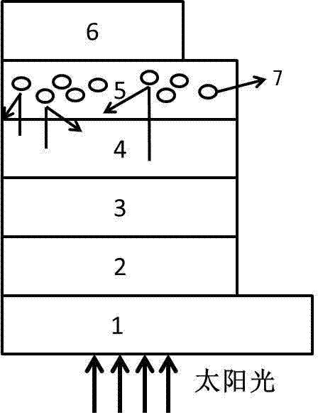
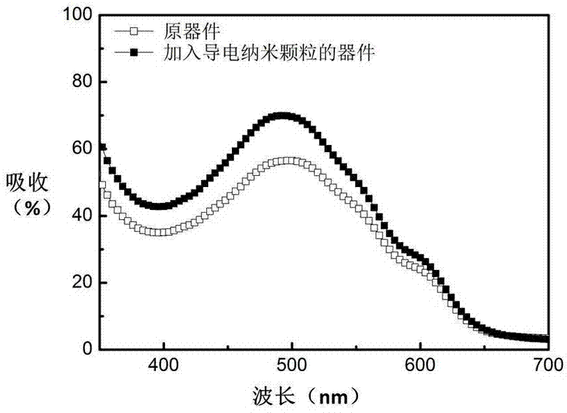
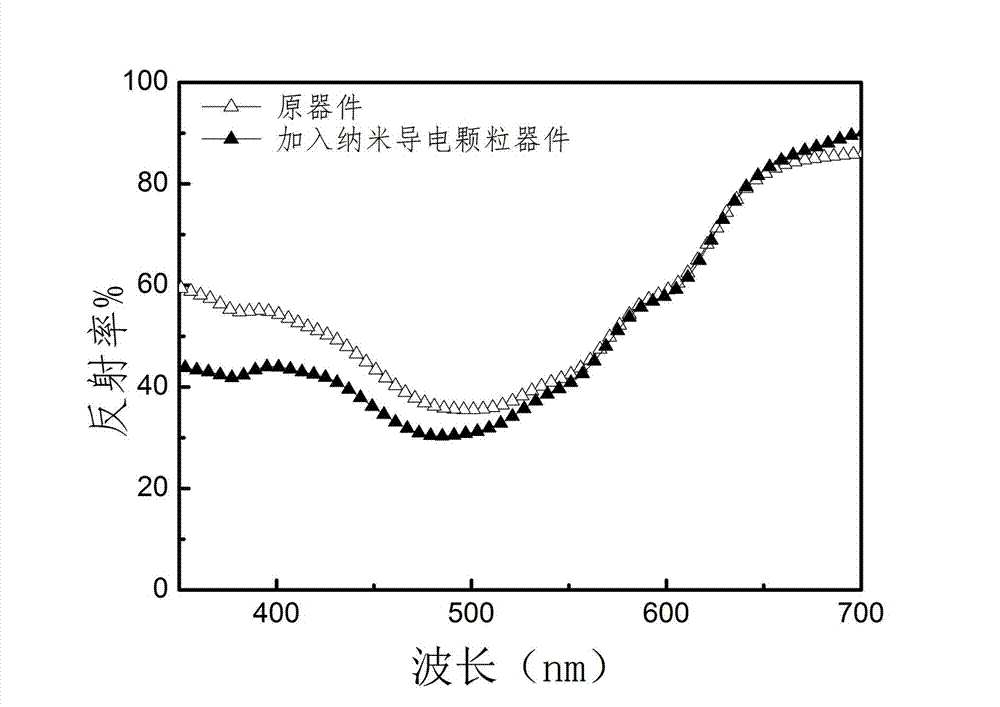
[0032] Embodiment 1: The substrate that the surface roughness is less than 1 nm is made up of transparent substrate and transparent conductive cathode ITO is cleaned, blows dry with nitrogen gas after cleaning; Spin-coat ZnO on the surface of transparent conductive cathode ITO (5000 rpm, 40 s, 15 nm), and the formed film was baked (200 ℃, 60 min); the photoactive layer of P3HT:PCBM (1:20, 20 mg / ml) was prepared by spin coating on the cathode buffer layer (1000 rpm, 25 s), and baked (140 ℃, 5 min); on the surface of the photoactive layer, spray the anode buffer layer mixed with transparent conductive nanoparticles (Ag nanoparticles, radius 30 nm, cyclohexane solvent) of PEDOT:PSS solution (transparent conductive nanoparticles 2%, dimethyl sulfoxide 5%, PEDOT:PSS 93%, 2500 rpm, 60 s, 15 nm); the substrate was annealed by heating and annealing on a constant temperature hot stage (150 ℃, 5 min); metal anode Ag (100 nm) was vapor-deposited on the anode buffer layer. Under standard...

Embodiment 2

[0033] Embodiment 2: the substrate that surface roughness is less than 1 nm is made up of transparent substrate and transparent conductive cathode ITO is cleaned, dry with nitrogen gas after cleaning; Spin-coat ZnO on the surface of transparent conductive cathode ITO (5000 rpm, 40 s, 20 nm), and the formed film was baked (200 ℃, 60 min); the photoactive layer of P3HT:PCBM (1:10, 10 mg / ml) was prepared by spin coating on the cathode buffer layer (1000 rpm, 25 s), and baked (140 ℃, 5 min); on the surface of the photoactive layer, spray the anode buffer layer doped with transparent conductive nanoparticles (Ag nanoparticles, radius 15 nm, cyclohexane solvent) of PEDOT:PSS solution (transparent conductive nanoparticles 5%, dimethyl sulfoxide 10%, PEDOT:PSS 85%, 2500 rpm, 50 s, 20 nm); the substrate was annealed by hot stage heating and annealing (170 ℃, 5 min ); the metal anode Ag (200 nm) was vapor-deposited on the anode buffer layer. Under standard test conditions: AM 1.5, 100 ...

Embodiment 3

[0034]Embodiment 3: The substrate that the surface roughness is less than 2 nm is made up of transparent substrate and transparent conductive cathode ITO is cleaned, dry with nitrogen gas after cleaning; Spin-coat ZnO on the surface of transparent conductive cathode ITO (5000 rpm, 40 s, 15 nm), and the formed film was baked (200 ℃, 60 min); the photoactive layer of P3HT:PCBM (1:10, 5 mg / ml) was prepared by spin coating on the cathode buffer layer (1000 rpm, 25 s), and baked (140 ℃, 5 min); on the surface of the photoactive layer, spray the anode buffer layer doped with transparent conductive nanoparticles (Ag nanoparticles, radius 60 nm, cyclohexane solvent) of PEDOT:PSS solution (transparent conductive nanoparticles 5%, dimethyl sulfoxide 7%, PEDOT:PSS 88%, 2500 rpm, 50 s, 20 nm); the substrate was annealed by heating and annealing on a constant temperature hot stage (150 ℃, 30 min); metal anode Ag (300 nm) was vapor-deposited on the anode buffer layer. Under standard test c...


PUM


Abstract

The invention discloses an inversed organic thin-film solar cell and a manufacturing method of the inversed organic thin-film solar cell. The inversed organic thin-film solar cell structurally and sequentially comprises a substrate, a transparent electric conduction cathode ITO, a cathode buffer layer, an optical activity layer, an anode buffer layer and a metallic cathode from bottom top top. Transparent electric conduction nano-particles are added in the anode buffer layer. The manufacturing method includes the steps of forming a substrate body through the substrate and the transparent electric conduction cathode ITO, washing and drying the base plate, manufacturing the cathode buffer layer on the surface of the transparent electric conduction cathode ITO, manufacturing and baking the optical activity layer on the surface of the cathode buffer layer, manufacturing the anode buffer layer on the surface of the optical activity layer, conducting annealing on the substrate body, and plating the anode buffer layer with the metallic cathode in an evaporation mode. High conductivity and high reflectivity of the transparent electric conduction nano-particles are used, the electron transmission rate and the light reflection rate of a traditional anode buffer layer are strengthened, the absorptivity of the optical activity layer to sunlight is improved, the light current density and the carrier transmission efficiency of the organic thin-film solar cell are accordingly improved, the series resistance of the cell is reduced, and the photoelectric conversion efficiency of a device is improved.

Description

technical field [0001] The invention belongs to the field of organic polymer photovoltaic devices or organic semiconductor thin-film solar cells, and in particular relates to an inverted organic thin-film solar cell and a preparation method thereof. Background technique [0002] With the explosive growth of the global energy demand, the energy problem has become the primary problem faced by the economic development of all countries. Because solar energy is clean, widely distributed, and inexhaustible, research on photovoltaic power generation to solve energy problems has become the focus and focus of research in the field of renewable energy. Currently, active layer materials can be classified into inorganic semiconductor materials and organic semiconductor materials according to the different properties of materials that make up the photoactive layer of a solar cell. Compared with inorganic semiconductor materials, organic semiconductor materials not only have relatively m...

Claims


Application Information

Patent Timeline
Patent Type & Authority Applications(China)
IPC IPC(8): H01L51/42H01L51/44H01L51/46H01L51/48
CPCY02E10/549H10K71/00H10K30/20H10K30/87
Inventor 于军胜郑毅帆李曙光施薇
Owner UNIV OF ELECTRONICS SCI & TECH OF CHINA
Why Eureka
Try Eureka