Boron diffusion method of N type silicon chip, crystalline silicon solar cell and manufacturing method of crystalline silicon solar cell

A diffusion method and a technology of silicon wafers, which are applied in semiconductor/solid-state device manufacturing, circuits, photovoltaic power generation, etc., can solve the problems of increasing the surface recombination rate, difficult control, complex process, etc., to reduce the surface recombination rate and improve conversion Efficiency, the effect of reducing boron source consumption

Active Publication Date: 2014-03-12
英辰新能源科技有限公司
View PDF6 Cites 10 Cited by
  • Summary
  • Abstract
  • Description
  • Claims
  • Application Information

AI Technical Summary

Problems solved by technology

However, the high-temperature deposition and high-temperature diffusion methods are complex and difficult to control, and the single-tube production capacity is low. The output of each furnace tube is only 80%, and the boron source consumption is relatively large. The excess boron source reacts with the quartz furnace tube to form A large amount of borosilicate glass (BGS) not only seriously corroded the diffusion furnace and other equipment, but also caused serious waste of boron source
The most important thing is that the uniformity of the diffusion square resistance obtained by the high-temperature deposition and high-temperature dif

Method used


Image

  • Boron diffusion method of N type silicon chip, crystalline silicon solar cell and manufacturing method of crystalline silicon solar cell
  • Boron diffusion method of N type silicon chip, crystalline silicon solar cell and manufacturing method of crystalline silicon solar cell
  • Boron diffusion method of N type silicon chip, crystalline silicon solar cell and manufacturing method of crystalline silicon solar cell

Examples


Embodiment 1

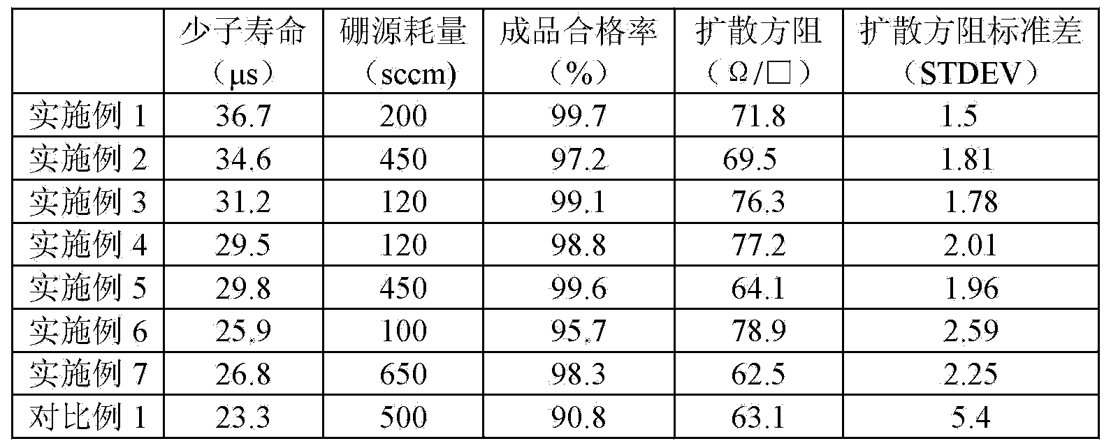
[0041] 1) Deposition stage: Take an N-type silicon wafer and carry out phosphorus diffusion and wet etching in sequence, and place the wet-etched silicon wafer (provided by Baoding Tianwei Yingli New Energy Co., Ltd.) in the furnace tube of the diffusion furnace. The silicon wafers are placed perpendicular to the quartz boat, and 500 wafers are placed in each furnace tube. Raise the temperature to 925°C at 10°C / min, feed in nitrogen, oxygen, and nitrogen carrying boron tribromide for reactive deposition for 25 minutes, wherein the oxygen flow rate is 65 sccm, the nitrogen flow rate carrying boron tribromide is 200 sccm, and the nitrogen flow rate is 22.5 slm .

[0042] 2) Diffusion stage: Stop feeding oxygen and boron sources, continue to feed nitrogen gas with a flow rate of 22.5 slm, and at the same time raise the temperature to 960°C at 10°C / min, and surface diffusion at 960°C for 25 minutes.

[0043] 3) Post-oxidation stage: Cool down the silicon wafer to 800°C (cool down...

Embodiment 2

[0046] 1) Deposition stage: Take an N-type silicon wafer and carry out phosphorus diffusion and wet etching in sequence, and place the wet-etched silicon wafer (provided by Baoding Tianwei Yingli New Energy Co., Ltd.) in the furnace tube of the diffusion furnace. The silicon wafers are placed perpendicular to the quartz boat, and 500 wafers are placed in each furnace tube. Raise the temperature to 900°C at 10°C / min, feed nitrogen, oxygen, and nitrogen carrying boron tribromide, wherein the flow rate of oxygen is 160 sccm, the flow rate of nitrogen carrying boron tribromide is 450 sccm, the flow rate of nitrogen gas is 23 slm, and the deposition time is 20 minute.

[0047] 2) Diffusion stage: Stop feeding oxygen and boron sources, continue to feed nitrogen gas with a flow rate of 23 slm, and at the same time raise the temperature to 950°C at 5°C / min, and diffuse on the surface at 950°C for 20 minutes.

[0048] 3) Post-oxidation stage: cool down the silicon wafer to 750°C (the ...

Embodiment 3

[0051] 1) Deposition stage: Take an N-type silicon wafer and carry out phosphorus diffusion and wet etching in sequence, and place the wet-etched silicon wafer (provided by Baoding Tianwei Yingli New Energy Co., Ltd.) in the furnace tube of the diffusion furnace. The silicon wafers are placed perpendicular to the quartz boat, and 500 wafers are placed in each furnace tube. Raise the temperature to 930°C at 10°C / min, feed nitrogen, oxygen, and nitrogen carrying boron tribromide, wherein the flow rate of oxygen is 30 sccm, the flow rate of nitrogen gas carrying boron tribromide is 120 sccm, the flow rate of nitrogen gas is 22 slm, and the deposition time is 30 minute.

[0052] 2) Diffusion stage: Stop feeding oxygen and boron sources, continue to feed nitrogen gas with a flow rate of 24 slm, and at the same time raise the temperature to 1000 °C at 15 °C / min, and diffuse on the surface at 1000 °C for 30 minutes.

[0053] 3) Post-oxidation stage: Cool down the silicon wafer to 85...


PUM


Abstract

The invention discloses a boron diffusion method of an N type silicon chip, a crystalline silicon solar cell and a manufacturing method of the crystalline silicon solar cell. The boron diffusion method comprises the following steps of a deposition stage: placing the silicon chip subjected to wet etching into a diffusion furnace, raising the temperature to a preset deposition temperature, and then introducing a boron source, oxygen and nitrogen for depositing the surface of the silicon chip; a diffusion promoting stage: raising the temperature of the silicon chip with the surface being deposited to a preset diffusion temperature for promoting the diffusion of boron, and introducing oxygen and nitrogen in the temperature raising and diffusion promoting processes; a post-oxidation stage: dropping the temperature of the diffused silicon chip, and introducing oxygen and nitrogen in the temperature dropping process. After the deposition diffusion process disclosed by the invention is adopted, the concentration of boron atoms on the surface of the silicon chip is reduced, the recombination rate and the lattice damage of the surface are reduced, the STDEV (standard deviation) is controlled to be about 2.0, the sheet resistance uniformity of boron diffusion is improved, the battery conversion efficiency is improved, the consumption of boron sources is also reduced, BGS (borosilicate glass) is prevented from being excessively generated, and the cost is reduced.

Description

technical field [0001] The invention relates to the technical field of solar cell manufacturing, in particular to a boron diffusion method for an N-type silicon wafer, a crystalline silicon solar cell and a manufacturing method thereof. Background technique [0002] Conventional fossil fuels are being exhausted day by day. Among the existing sustainable energy sources, solar energy is undoubtedly the cleanest, most common and most potential alternative energy source. At present, among all solar cells, silicon solar cells are one of the solar cells that have been widely commercialized. This is due to the extremely abundant reserves of silicon materials in the earth's crust. With excellent electrical and mechanical properties, silicon solar cells occupy an important position in the field of photovoltaics. Therefore, developing cost-effective silicon solar cells has become one of the main research directions of photovoltaic companies in various countries. [0003] In the prod...

Claims


Application Information

Patent Timeline
IPC IPC(8): H01L21/22H01L31/18H01L31/068
CPCY02E10/50Y02E10/547Y02P70/50
Inventor 袁广锋何广川陈艳涛李雪涛
Owner 英辰新能源科技有限公司
Why Eureka
Try Eureka