

Method for manufacturing and repairing conducting circuits on surfaces of ceramic substrates
A technology of ceramic substrates and conductive circuits, which is applied in the manufacture of printed circuits, the improvement of the metal adhesion of insulating substrates, printed circuits, etc., can solve the problems of low graphic accuracy, difficult industrial application, low degree of flexibility, etc., and achieve repeatability and The effect of high quality stability, large-format three-dimensional processing, and high degree of flexibility
- Summary
- Abstract
- Description
- Claims
- Application Information
AI Technical Summary
Problems solved by technology
Method used
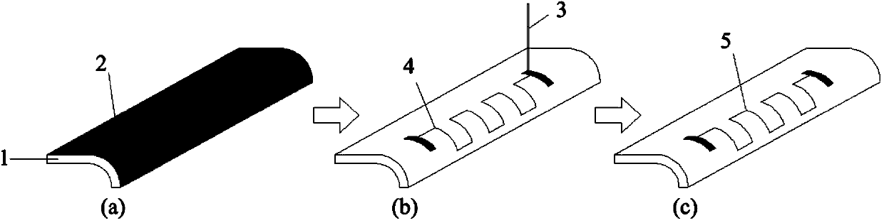
Image


Examples
Embodiment 1
[0045] The whole 99% alumina ceramic sheet was soaked in an aqueous solution containing 0.1 mol / L nickel ions, the soaking temperature was room temperature, and the soaking time was 5 minutes, and then it was taken out and dried. After that, the 99% alumina ceramic sheet was fixed on the table of the three-axis CNC machine tool, and the pulse CO with the maximum output power of 100W was used. 2 The laser and laser scanning galvanometer scan the surface of the substrate according to the 1.2mm×23mm rectangular electrode pattern designed and generated by the CAD software. The laser power is 20W, the pulse frequency is 5KHz, the scanning speed is 600mm / s, the width of the single scanning line is 100μm, and the spacing between the scanning lines is 100 μm. 100μm (at this time, the laser power density is 2.55×10 5 W / cm 2 ). Next, the substrate was ultrasonically cleaned in deionized water to remove nickel ions from the surface of the non-laser treated areas. After that, the above...
Embodiment 2
[0047] An aqueous solution containing 0.5 mol / L palladium ion and palladium ammine ion was coated on the position of the designed circuit pattern on the surface of 96% alumina ceramic, and dried. Afterwards, the 96% alumina ceramic was fixed on the table of the three-axis linkage CNC machine tool, and the surface of the substrate was scanned according to the circuit pattern generated by the CAD software using a continuous fiber laser with a maximum output power of 20W and a wavelength of 1064nm and a laser scanning galvanometer. The laser power is 10w, the scanning speed is 200mm / s, the width of the single scanning line is 20μm, and the spacing between the scanning lines is 20μm (at this time, the laser power density is 3.18×10 6 W / cm 2 ). Next, the substrate is placed in deionized water and ultrasonically cleaned to remove palladium ions and palladium ammonia ions on the surface of the untreated area. After that, the above-mentioned substrate was put into an electroless pla...
Embodiment 3
[0049] The ring-shaped strontium titanate ceramic was soaked in an aqueous solution of 0.3 mol / L iron ions, the soaking temperature was room temperature, and the soaking time was 5 minutes, and then it was taken out and dried. Then, the ring-shaped strontium titanate ceramic was fixed on the table of the three-axis CNC machine tool, and the pulsed Nd:YVO with the maximum output power of 10W and the wavelength of 355nm was used. 4 The laser and laser scanning galvanometer scan the surface of the substrate according to the circuit pattern generated by the CAD software. The laser power is 3W, the scanning speed is 800mm / s, the width of the single scanning line is 10μm, and the spacing between the scanning lines is 10μm (the power density of the laser is 3.82 at this time). ×10 6 W / cm 2 ). The substrate is next cleaned to remove iron ions from the surface of the unlasered areas. After that, the above-mentioned substrate was put into an electroless plating solution for electrole...
PUM
| Property | Measurement | Unit |
|---|---|---|
| Thickness | aaaaa | aaaaa |
| Resistivity | aaaaa | aaaaa |
| Thickness | aaaaa | aaaaa |
Abstract
Description
Claims
Application Information