Method for preparing PID-resisting film

A thin-film and double-film technology, which is applied in final product manufacturing, sustainable manufacturing/processing, photovoltaic power generation, etc., can solve the problems of increased battery failure rate, increased control difficulty, poor PID performance, etc., and achieves obvious results. Easy to operate, simple process effect

Inactive Publication Date: 2014-07-23
JA SOLAR TECH YANGZHOU
View PDF4 Cites 7 Cited by
  • Summary
  • Abstract
  • Description
  • Claims
  • Application Information

AI Technical Summary

Problems solved by technology

The client’s SunEdison power station system has been used for less than a year, and the power output of some components is lower than 80%, complaining about poor PID performance; the more commonly used anti-PID preparation method is mainly to use homogeneous silicon nitride film, using high and low refractive index In the process of battery preparation, due to the difficulty of machine control due to the higher refractive index, the failure rate of the battery increases, and the photoelectric conversion efficiency of the solar cell decreases by about 0.3%.

Method used


Image

  • Method for preparing PID-resisting film

Examples


Embodiment 1

[0016] For a 156x156mm polysilicon wafer, the preparation process of this embodiment is as follows:

[0017] (1) On the light-receiving surface of the silicon wafer after conventional texturing and diffusion, UV equipment (CDA flow rate 5slm, lamp power 20%, temperature: 25°C) is used to prepare a silicon wafer with a thickness of 2nm and a refractive index on the surface of the silicon wafer. 1.46 silicon oxide film;

[0018] (2) On the silicon oxide film, use the seven-star tube PECED equipment to deposit a silicon nitride film under the conditions of a temperature of 450°C, a total flow rate of ammonia and silane of 7000SCCM, and a power of 6500W. The specific film thickness range is controlled at 70nm, and the refractive index is controlled. In 2.10.

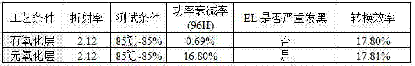
[0019] (3) The film thickness of the prepared silicon oxide and silicon nitride double-layer film is 82nm, and the refractive index is 2.12; and then a solar cell is made through a follow-up conventional process. The perfor...

Embodiment 2

[0024] For a 156x156mm polysilicon wafer, the preparation process of this embodiment is as follows:

[0025] (1) On the silicon wafer after conventional texturing and diffusion, the seven-star tube PECVD is adopted to use the seven-star tube PECVD with high RF power (about 5.5kw), N 2 O:SiH 4 The volume ratio is 7:1, and the silicon oxide film is prepared on the surface of the silicon wafer, the film thickness is controlled at 25nm, and the refractive index is controlled at 1.6;

[0026] (2) On the silicon oxide or silicon oxynitride film, use seven-star tube PECVD with high RF power (about 7kw), NH 3 :SiH 4 =7:1, the silicon nitride film thickness is controlled at 55nm, and the refractive index is controlled at 2.08;

[0027] (3) The total film thickness of the prepared silicon oxide thin film and silicon nitride thin film bilayer film is 82 nm, and the refractive index is 2.12.

[0028]


PUM

PropertyMeasurementUnit
thicknessaaaaaaaaaa
thicknessaaaaaaaaaa
thicknessaaaaaaaaaa

Abstract

The invention discloses a method for preparing a PID-resisting film. The method includes the following steps that a crystal silicon wafer is selected, after texturing and diffusing are performed, double layers of films of a silicon oxide film and a silicon nitride film or a silicon oxynitride film and a silicon nitride film are sequentially generated on a light receiving face of the crystal silicon wafer. The silicon oxide film is deposited in an ultraviolet photosensitized oxidation mode or a PECVD mode, silicon nitride or silicon oxynitride is deposited in a PECVD mode, silicon oxide or the silicon oxynitride located at a bottom layer has the blocking action on foreign ions, the passivation effect is good, the silicon nitride film located on a top layer is combined, losses of the photoelectric conversion efficiency of solar cell pieces can be reduced, and the PID-resisting performance of the solar cell pieces can be enhanced.

Description

technical field [0001] The invention belongs to the technical field of solar cell manufacturing, and in particular relates to a method for preparing an anti-PID thin film. Background technique [0002] Crystalline silicon solar cells do not emit or emit any harmful substances during use; there are no moving parts, no noise, light weight, small size, modular features, can be dispersed and set up on site, the construction period is short, and the working life is long 20-25 Years, easy maintenance, reliable operation and other advantages, it is a very ideal renewable clean energy. In practical applications, because the output voltage and power of a single crystalline silicon solar module are too low to meet the needs of life or production, multiple modules need to be connected in series. Under the condition that the outer frame is grounded, multiple components connected in series will result in high reverse bias voltage between the outer frame and the surface of the cell. In ...

Claims


Application Information

Patent Timeline
Patent Type & Authority Applications(China)
IPC IPC(8): H01L31/18
CPCH01L31/02167H01L31/1868Y02E10/50Y02P70/50
Inventor 闫用用张惠张亮苗青李积伟
Owner JA SOLAR TECH YANGZHOU
Why Eureka
Try Eureka