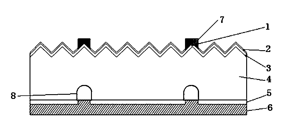
Manufacturing method for PERL crystalline silicon solar cell capable of being massively produced
A technology of solar cells and manufacturing methods, applied in the direction of final product manufacturing, sustainable manufacturing/processing, circuits, etc., can solve problems such as undetermined process methods, achieve the effects of reducing equipment investment, increasing manufacturing costs, and saving costs
- Summary
- Abstract
- Description
- Claims
- Application Information
AI Technical Summary
Problems solved by technology
Method used
Image
Examples
Embodiment 1
[0040] A kind of manufacturing method of the PERL crystalline silicon solar cell of mass production, comprises the following steps:
[0041] (1) Silicon wafers are damaged, textured and cleaned:
[0042] A 156mm P-type single crystal silicon wafer is selected as the base material, and its resistivity is 1 ohm cm. After removing damage to the selected p-type silicon wafer, use 0.5% sodium hydroxide or potassium hydroxide solution at 75°C Perform chemical etching on the surface of the P-type silicon wafer to prepare a pyramid-shaped suede surface, and then clean it with 1% hydrofluoric acid to remove impurities;
[0043] (2) Phosphorus diffusion: adopt the method of tubular phosphorus diffusion, specifically in the diffusion furnace at a temperature of 600 ° C, using POCl 3 Phosphorus is diffused on the front side of the silicon wafer to form an n-type layer, so that the square resistance of P-type crystalline silicon is 25ohm / sq, and the naturally formed phosphosilicate glass ...
Embodiment 2
[0056] A kind of manufacturing method of the PERL crystalline silicon solar cell of mass production, comprises the following steps:
[0057] (1) Silicon wafers are damaged, textured and cleaned:
[0058] Select a 156mm P-type single crystal silicon wafer as the base material, and its resistivity is 2 ohm·cm. After removing the damage of the selected p-type silicon wafer, use 1% sodium hydroxide or potassium hydroxide solution at 80°C Perform chemical etching on the surface of the P-type silicon wafer to prepare a pyramid-shaped suede surface, and then clean it with hydrofluoric acid with a mass fraction of 5% to remove impurities;
[0059] (2) Phosphorus diffusion: adopt the method of tubular phosphorus diffusion, specifically in the diffusion furnace at a temperature of 750 ° C, using POCl 3 Phosphorus is diffused on the front side of the silicon wafer to form an n-type layer, so that the square resistance of P-type crystalline silicon is 100ohm / sq, and the naturally formed ...
Embodiment 3
[0072] A kind of manufacturing method of the PERL crystalline silicon solar cell of mass production, comprises the following steps:
[0073] (1) Silicon wafers are damaged, textured and cleaned:
[0074] A 156mm P-type single crystal silicon wafer is selected as the base material, and its resistivity is 3 ohm cm. After removing damage to the selected p-type silicon wafer, use 2% sodium hydroxide or potassium hydroxide solution at 85°C Perform chemical etching on the surface of the P-type silicon wafer to prepare a pyramid-shaped suede surface, and then clean it with 15% hydrofluoric acid to remove impurities;
[0075] (2) Phosphorus diffusion: adopt the method of tubular phosphorus diffusion, specifically in the diffusion furnace at a temperature of 800 ° C, using POCl 3 Phosphorus is diffused on the front side of the silicon wafer to form an n-type layer, so that the square resistance of P-type crystalline silicon is 150ohm / sq, and the naturally formed phosphosilicate glass ...
PUM
| Property | Measurement | Unit |
|---|---|---|
| Square resistance | aaaaa | aaaaa |
| Thickness | aaaaa | aaaaa |
| Thickness | aaaaa | aaaaa |
Abstract
Description
Claims
Application Information
 - Generate Ideas
- Intellectual Property
- Life Sciences
- Materials
- Tech Scout
- Unparalleled Data Quality
- Higher Quality Content
- 60% Fewer Hallucinations
Browse by: Latest US Patents, China's latest patents, Technical Efficacy Thesaurus, Application Domain, Technology Topic, Popular Technical Reports.
© 2025 PatSnap. All rights reserved.Legal|Privacy policy|Modern Slavery Act Transparency Statement|Sitemap|About US| Contact US: help@patsnap.com

