Preparation method of nanoimprint nickel seal
A technology of nano-imprinting and stamping, which is applied in nano-technology, photo-engraving process of patterned surface, originals for opto-mechanical processing, etc. , to achieve the effect of low price
- Summary
- Abstract
- Description
- Claims
- Application Information
AI Technical Summary
Problems solved by technology
Method used
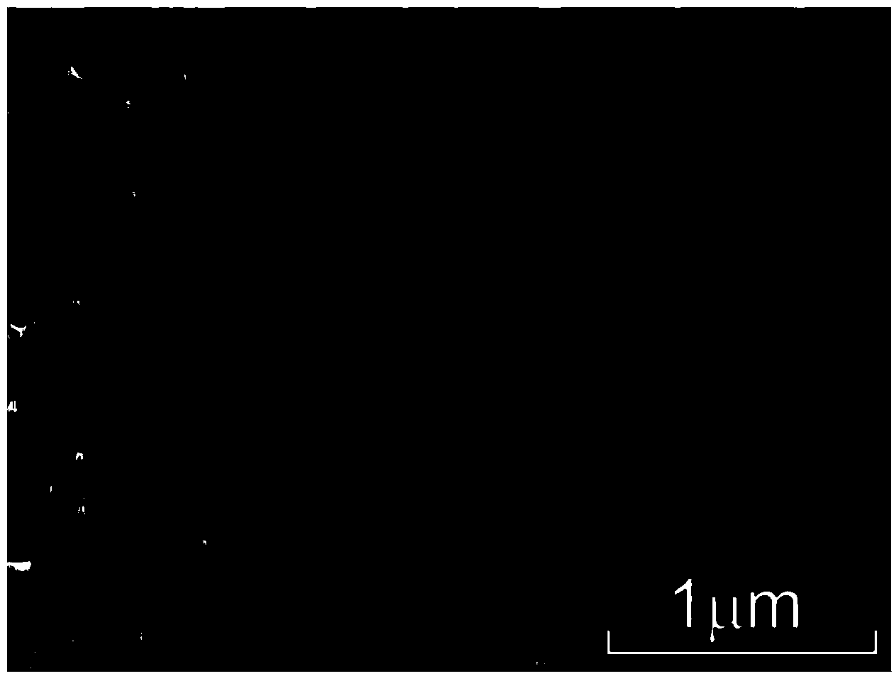
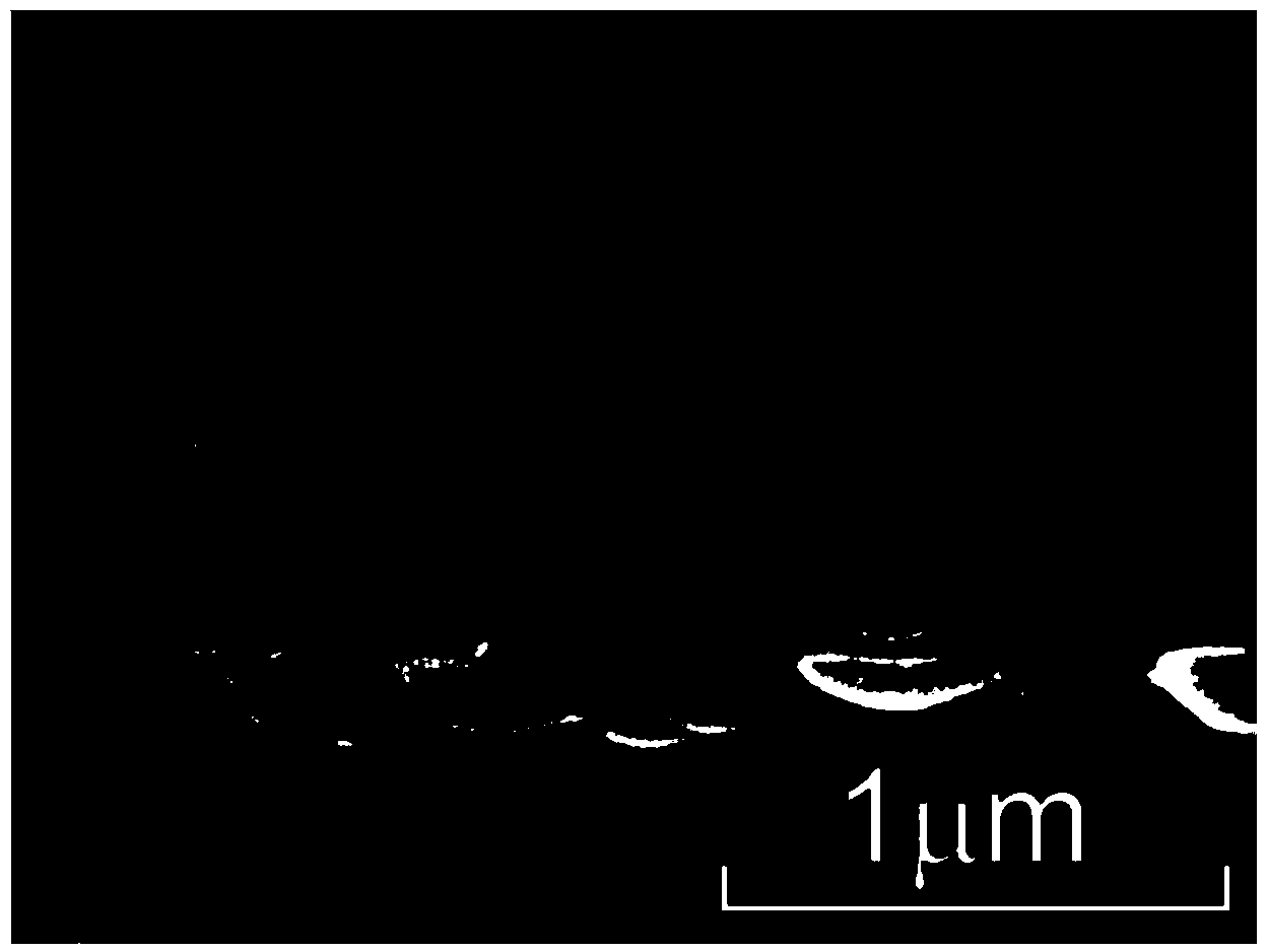
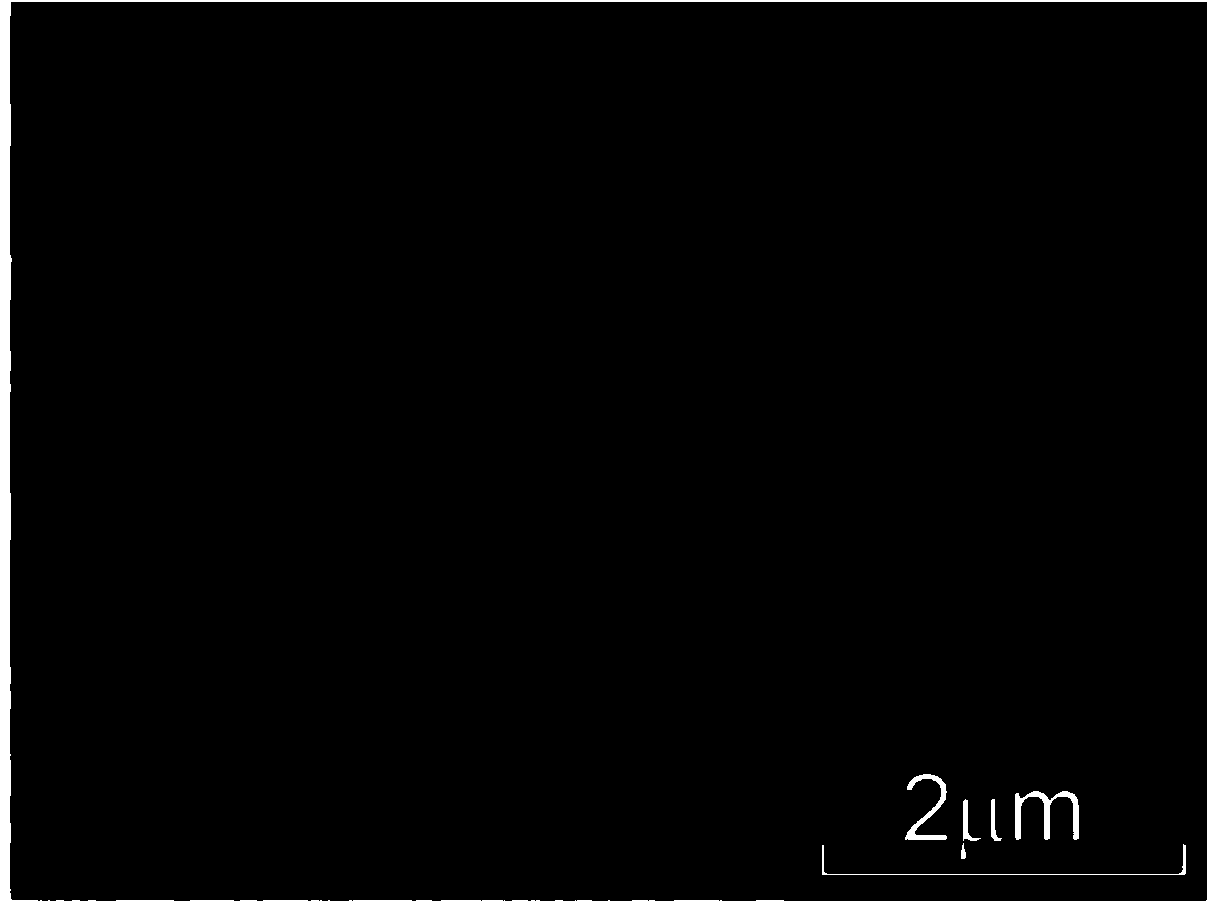
Image

Examples
Embodiment 1
[0041] The aluminum material is degreased, surface cleaned, and polished using conventional methods; in a 5% (mass percent) phosphoric acid electrolyte, the aluminum material is used as the anode and the graphite is the cathode, and the aluminum material is subjected to constant-voltage anodic oxidation by a voltage source. 0°C, a voltage of 200V, and a time of 10 hours to obtain an anodic aluminum oxide film with a thickness of 60 microns; in phosphoric acid (H 3 PO 4 ) and 30g / L of chromium trioxide (CrO 3 ) in the mixed solution of chemical corrosion to completely remove the anodic aluminum oxide film at a temperature of 70°C; carry out constant voltage anodic oxidation on the aluminum material after removing the aluminum oxide film at a temperature of 0°C and a voltage of 200V for 5 minutes to obtain Thickness is the anodic aluminum oxide film of 300 nanometers, and in 5% (mass percent) phosphoric acid, 30 ℃ down hole expansion 40 minutes, obtain the anodic aluminum oxide...
Embodiment 2
[0044] The aluminum material is degreased, surface cleaned, and polished using conventional methods; the aluminum material is subjected to constant voltage anodization in a 10% (mass percentage) phosphoric acid electrolyte, the temperature is 10°C, the voltage is 150V, and the time is 6 hours. Obtain the anodic aluminum oxide film that thickness is 10 microns; Be that the phosphoric acid (H of 50mL / L 3 PO 4 ) and 30g / L of chromium trioxide (CrO 3 ) in the mixed solution of chemical corrosion to completely remove the anodic aluminum oxide film at a temperature of 70°C; carry out constant voltage anodic oxidation on the aluminum material after the aluminum oxide film has been removed at a temperature of 10°C and a voltage of 150V for 5 minutes, and then In 5% (mass percentage) phosphoric acid, 30 ℃ under expansion hole 10 minutes; Repeat anodic oxidation, chemical corrosion, hole expansion process 4 times, obtain the anodized aluminum film with the tapered hole that thickness i...
Embodiment 3
[0046] The aluminum material is degreased, surface cleaned, and polished using conventional methods; in a 1% (mass percentage) phosphoric acid electrolyte, the aluminum material is used as the anode and the graphite is the cathode, and the aluminum material is subjected to constant voltage anodic oxidation by a voltage source. 0°C, a voltage of 100V, and a time of 10 hours to obtain an anodic aluminum oxide film; in phosphoric acid (H 3 PO 4 ) and 30g / L of chromium trioxide (CrO 3 ) in the mixed solution of chemical corrosion to completely remove the anodic aluminum oxide film at a temperature of 70°C; carry out constant voltage anodic oxidation on the aluminum material after the removal of the aluminum oxide film at a temperature of 0°C and a voltage of 100V for 20 minutes to obtain Anodized aluminum film, and in 30% (mass percentage) phosphoric acid 0 ℃ down hole expansion 40 minutes, obtain the anodized aluminum film with conical hole; Make the anodized aluminum film obtai...
PUM
| Property | Measurement | Unit |
|---|---|---|
| thickness | aaaaa | aaaaa |
| thickness | aaaaa | aaaaa |
Abstract
Description
Claims
Application Information
 - R&D
- Intellectual Property
- Life Sciences
- Materials
- Tech Scout
- Unparalleled Data Quality
- Higher Quality Content
- 60% Fewer Hallucinations
Browse by: Latest US Patents, China's latest patents, Technical Efficacy Thesaurus, Application Domain, Technology Topic, Popular Technical Reports.
© 2025 PatSnap. All rights reserved.Legal|Privacy policy|Modern Slavery Act Transparency Statement|Sitemap|About US| Contact US: help@patsnap.com