Light-emitting diode epitaxial slice and manufacturing method thereof

A technology of light-emitting diodes and epitaxial wafers, which is applied in the direction of electrical components, circuits, semiconductor devices, etc., can solve the problems of inability to withstand large currents, poor reliability, and high voltage, so as to prevent negative effects on crystal quality, increase recombination probability, and prolong use. The effect of longevity

Active Publication Date: 2014-10-08
HC SEMITEK SUZHOU
View PDF6 Cites 11 Cited by
  • Summary
  • Abstract
  • Description
  • Claims
  • Application Information

AI Technical Summary

Problems solved by technology

[0006] In order to solve the problems of high voltage, inability to withstand high current, and poor reliability in the prior art, an embodiment of the present invention provides a light-emitting diode epitaxial wafer and a manufacturing method thereof

Method used


Image

  • Light-emitting diode epitaxial slice and manufacturing method thereof
  • Light-emitting diode epitaxial slice and manufacturing method thereof
  • Light-emitting diode epitaxial slice and manufacturing method thereof

Examples


Embodiment 1

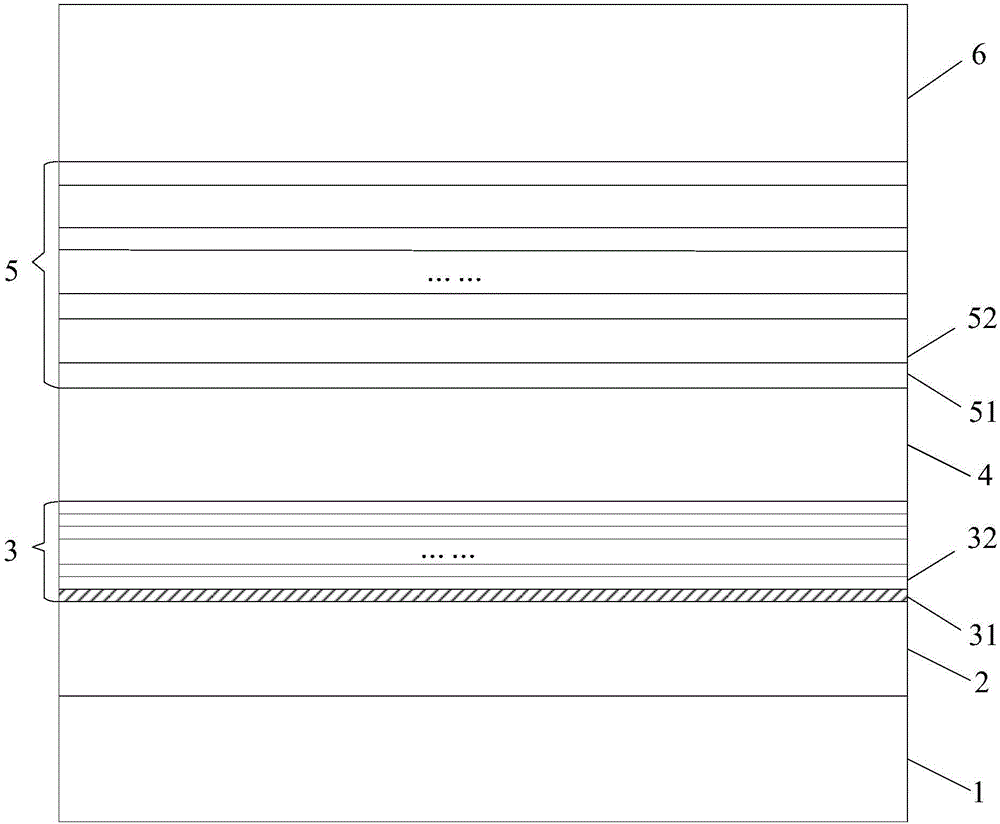
[0030] An embodiment of the present invention provides an LED epitaxial wafer, see figure 1 , the epitaxial wafer includes a substrate 1 , and a low-temperature buffer layer 2 , a high-temperature buffer layer 3 , an N-type layer 4 , an active layer 5 , and a P-type layer 6 stacked on the substrate 1 in sequence.

[0031] In this embodiment, the high-temperature buffer layer includes at least two GaN layers, the Si doping concentration of the at least two GaN layers increases from 0 along the growth direction of the epitaxial wafer layer by layer, and the Si doping concentration of the at least two GaN layers Both are less than the Si doping concentration of the N-type layer.

[0032] Optionally, the thickness of the first GaN layer 31 is greater than or equal to the total thickness of all the second GaN layers 32 . Wherein, the first GaN layer 31 is a GaN layer ( figure 1 ), the second GaN layer 32 is a GaN layer with a Si doping concentration greater than zero in at least ...

Embodiment 2

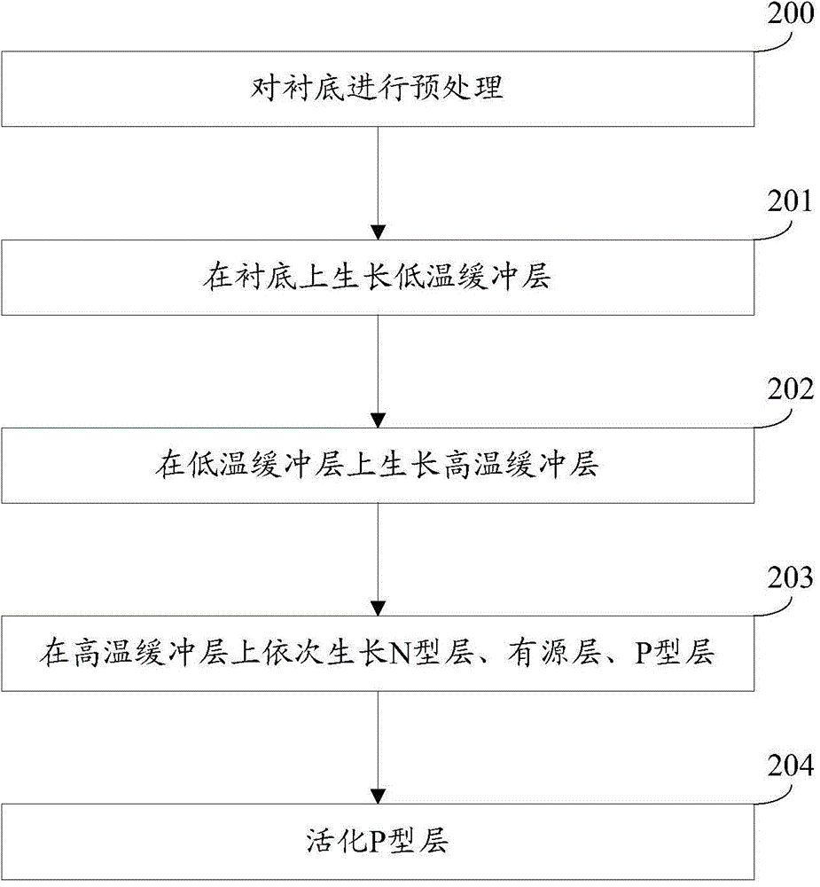
[0044] An embodiment of the present invention provides a method for manufacturing an LED epitaxial wafer, the method is used to manufacture the LED epitaxial wafer as described in Embodiment 1, see figure 2 , the method includes:

[0045] Step 200: Perform pretreatment on the substrate.

[0046] In this embodiment, Veeco K465i MOCVD (Metal Organic Chemical Vapor Deposition, Metal Organic Compound Chemical Vapor Deposition) is used to realize the manufacturing method of the LED epitaxial wafer. Using high-purity H 2 (hydrogen) or high-purity N 2 (nitrogen) or high purity H 2 and high purity N 2 The mixed gas as the carrier gas, high-purity NH 3 As the N source, trimethylgallium (TMGa) and triethylgallium (TEGa) are used as the gallium source, trimethylindium (TMIn) is used as the indium source, silane (SiH4) is used as the N-type dopant, and trimethylaluminum ( TMAl) as an aluminum source, magnesium dicene (CP 2 Mg) as a P-type dopant.

[0047] Optionally, the substrat...


PUM


Abstract

The invention discloses a light-emitting diode epitaxial slice and a manufacturing method thereof and belongs to the technical field of semiconductors. The epitaxial slice comprises a substrate, a low-temperature buffer layer, a high-temperature buffer layer, an N-type layer, an active layer and a P-type layer, wherein the low-temperature buffer layer, the high-temperature buffer layer, the N-type layer, the active layer and the P-type layer are sequentially laminated on the substrate. The high-temperature buffer layer comprises at least two GaN layers, and the Si doping concentration of the at least two GaN layers is increased layer by layer from 0 in the growth direction of the epitaxial slice and is smaller than that of the N-type layer. By increasing the Si doping concentration of the at least two GaN layers layer by layer from 0 in the growth direction of the epitaxial slice, electrons can be effectively provided, a current expanding area is increased, the current expansibility is improved, electron injection efficiency is improved, the probability of recombination of the electrons and holes is improved, resistance in a high-power chip is reduced, chip voltage is greatly reduced, the capability chip of resisting a high current is improved, and chip reliability is improved.

Description

technical field [0001] The invention relates to the technical field of semiconductors, in particular to a light-emitting diode epitaxial wafer and a manufacturing method thereof. Background technique [0002] LED (Light Emitting Diode, Light Emitting Diode) is a semiconductor electronic component that can emit light. As a new type of high-efficiency, environmentally friendly and green solid-state lighting source, LED has the advantages of low voltage, low power consumption, small size, light weight, long life, high reliability, etc., and is being rapidly and widely used, such as traffic lights, automobiles, etc. Interior and exterior lights, urban landscape lighting, mobile phone backlight, outdoor full-color display, etc. [0003] High-power chips are LED chips with light source power greater than or equal to 350mw. Existing LED epitaxial wafers for making high-power chips include a substrate, and a low-temperature buffer layer, a high-temperature buffer layer, an N-type ...

Claims


Application Information

Patent Timeline
Patent Type & Authority Applications(China)
IPC IPC(8): H01L33/14H01L33/12H01L33/00
CPCH01L33/007H01L33/12H01L33/14
Inventor 姚振从颖韩杰胡加辉魏世祯
Owner HC SEMITEK SUZHOU
Why Eureka
Try Eureka