
ZnO/NiO heterostructure orderly multi-hole thin film and manufacturing method thereof

A porous film and heterostructure technology, applied in the semiconductor field, can solve the problems of semiconductor devices that have not been reported, and achieve the effect of improving the overall performance, good resistive characteristics, and obvious rectification characteristics

Active Publication Date: 2015-03-25
SOUTHWEST UNIVERSITY
View PDF5 Cites 8 Cited by
  • Summary
  • Abstract
  • Description
  • Claims
  • Application Information

AI Technical Summary

Problems solved by technology

At present, there is no report on the semiconductor device prepared by ZnO / NiO heterostructure ordered porous film

Method used


Image

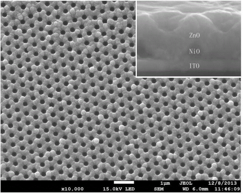
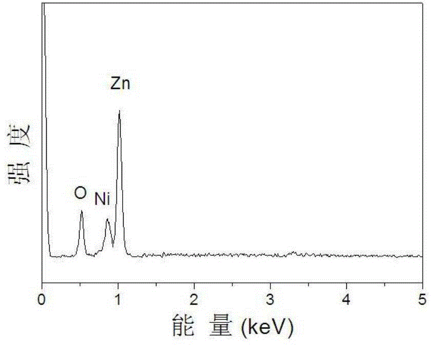
  • ZnO/NiO heterostructure orderly multi-hole thin film and manufacturing method thereof
  • ZnO/NiO heterostructure orderly multi-hole thin film and manufacturing method thereof
  • ZnO/NiO heterostructure orderly multi-hole thin film and manufacturing method thereof

Examples


Embodiment 1

[0027] Example 1 Preparation of ZnO / NiO Heterostructure Ordered Porous Film

[0028] Step 1, first place the single-layer colloidal crystal template composed of polystyrene colloidal spheres with a diameter of 500nm on the conductive glass, and then place the conductive substrate with the single-layer colloidal crystal template on it in the nickel electrolyte to It is the working electrode, graphite is the counter electrode, and the current density is 1.0mA / cm 2 Electrodeposition by the two-electrode method was carried out for 5 minutes to obtain an ordered porous film of metallic nickel;

[0029] Step 2, place the conductive substrate grown on the ordered porous film of metallic nickel in a high-temperature tube furnace for thermal oxidation treatment, during which the high-purity O 2 The flow rate is 30sccm, the heating rate is 2°C / min, and the temperature is raised to 500°C. After maintaining the temperature for 3 hours, it is naturally cooled to room temperature. The coll...

Embodiment 2

[0034] Example 2 Preparation of ZnO / NiO Heterostructure Ordered Porous Film

[0035] Step 1, first place a single-layer colloidal crystal template composed of polystyrene colloidal spheres with a diameter of 500nm on a conductive glass substrate, and then place the conductive substrate with a single-layer colloidal crystal template on it in a nickel electrolyte , using it as the working electrode and graphite as the counter electrode, at a current density of 1.5mA / cm 2 The ordered porous film of metallic nickel was obtained by electrodepositing for 4 minutes by the two-electrode method;

[0036] Step 2, place the conductive substrate grown on the ordered porous film of metallic nickel in a high-temperature tube furnace for thermal oxidation treatment, during which the high-purity O 2 The flow rate is 40sccm, the heating rate is 4°C / min, and the temperature is raised to 500°C. After maintaining the temperature for 4 hours, it is naturally cooled to room temperature. The colloi...

Embodiment 3

[0039] Example 3 Preparation of ZnO / NiO Heterostructure Ordered Porous Film

[0040] Step 1, first place a single-layer colloidal crystal template composed of polystyrene colloidal spheres with a diameter of 500nm on a silicon wafer coated with an ITO conductive layer, and then place a conductive substrate with a single-layer colloidal crystal template on it. In the nickel electrolyte, use it as the working electrode and graphite as the counter electrode, at a current density of 2.0mA / cm 2 The ordered porous film of metallic nickel was obtained by electrodepositing for 4 minutes by the two-electrode method;

[0041] Step 2, place the conductive substrate grown on the ordered porous film of metallic nickel in a high-temperature tube furnace for thermal oxidation treatment, during which the high-purity O 2 The flow rate is 40sccm, the heating rate is 3°C / min, and the temperature is raised to 400°C. After maintaining the temperature for 3 hours, it is naturally cooled to room te...


PUM

PropertyMeasurementUnit
diameteraaaaaaaaaa
thicknessaaaaaaaaaa
diameteraaaaaaaaaa

Abstract

The invention belongs to the technical field of semiconductors and particularly relates to a ZnO / NiO heterostructure orderly multi-hole thin film and a manufacturing method thereof. A new option is provided for semiconductor materials. According to the technical scheme, the ZnO / NiO heterostructure orderly multi-hole thin film comprises a conducting substrate and a heterostructure growing on the conducting substrate, and the heterostructure is formed by a p type NiO orderly multi-hole thin film and an n type ZnO orderly multi-hole thin film which grows in sequence from bottom to top. The invention further provides a manufacturing method of the ZnO / NiO heterostructure orderly multi-hole thin film. The ZnO / NiO heterostructure orderly multi-hole thin film can be widely used in the fields such as an ultraviolet detector, a light-emitting diode and a resistance random access memory.

Description

technical field [0001] The invention belongs to the technical field of semiconductors, and in particular relates to a ZnO / NiO heterostructure ordered porous film and a preparation method thereof. Background technique [0002] ZnO is a new type of wide band gap (3.37 eV) semiconductor material with excellent photoconductive properties and resistance transition properties. Compared with other wide band gap materials, it has better resistance to high-energy ray radiation and good thermal stability. , chemical stability, and easy access to raw materials, which is conducive to the production of high-performance ultraviolet detection devices and resistive memory devices, and has become a hot spot in the field of semiconductor research. [0003] The semiconductor pn junction ultraviolet detector has the advantages of low dark current, fast response speed, and zero-bias operation, and has become a more commonly used ultraviolet detector structure at present. In addition, studies ha...

Claims


Application Information

Patent Timeline
Patent Type & Authority Applications(China)
IPC IPC(8): H01L45/00H01L33/02H01L31/109H01L33/00H01L31/18C23C28/04
CPCY02P70/50
Inventor 赵建伟秦丽溶贾小亚杨彩风
Owner SOUTHWEST UNIVERSITY
Learn More