Supercharge Your Innovation With Domain-Expert AI Agents!

Method for preparing microfluidic doped nanocrystal lasers using femtosecond pulsed laser

A femtosecond pulse, micro-channel technology, applied in the manufacture of micro-structure devices, processes for producing decorative surface effects, micro-structure technology, etc., can solve the problems of complicated design and preparation of micro-channel chips, and achieve laser medium Diversification, strong controllability, simple process and environmental protection effect

Inactive Publication Date: 2017-11-28
SICHUAN UNIV
View PDF8 Cites 0 Cited by
  • Summary
  • Abstract
  • Description
  • Claims
  • Application Information

AI Technical Summary

Problems solved by technology

However, the microfluidic chip lasers with the above two structures are somewhat cumbersome in the design and preparation of the microfluidic chip, and only laser dyes are used as the laser medium, which fails to give full play to the characteristics of its micro-device. Based on this, the research group proposed A preparation method of a microchannel-doped nanocrystal laser device with a simple preparation method and diverse laser media

Method used


Image

  • Method for preparing microfluidic doped nanocrystal lasers using femtosecond pulsed laser
  • Method for preparing microfluidic doped nanocrystal lasers using femtosecond pulsed laser
  • Method for preparing microfluidic doped nanocrystal lasers using femtosecond pulsed laser

Examples


Embodiment 1

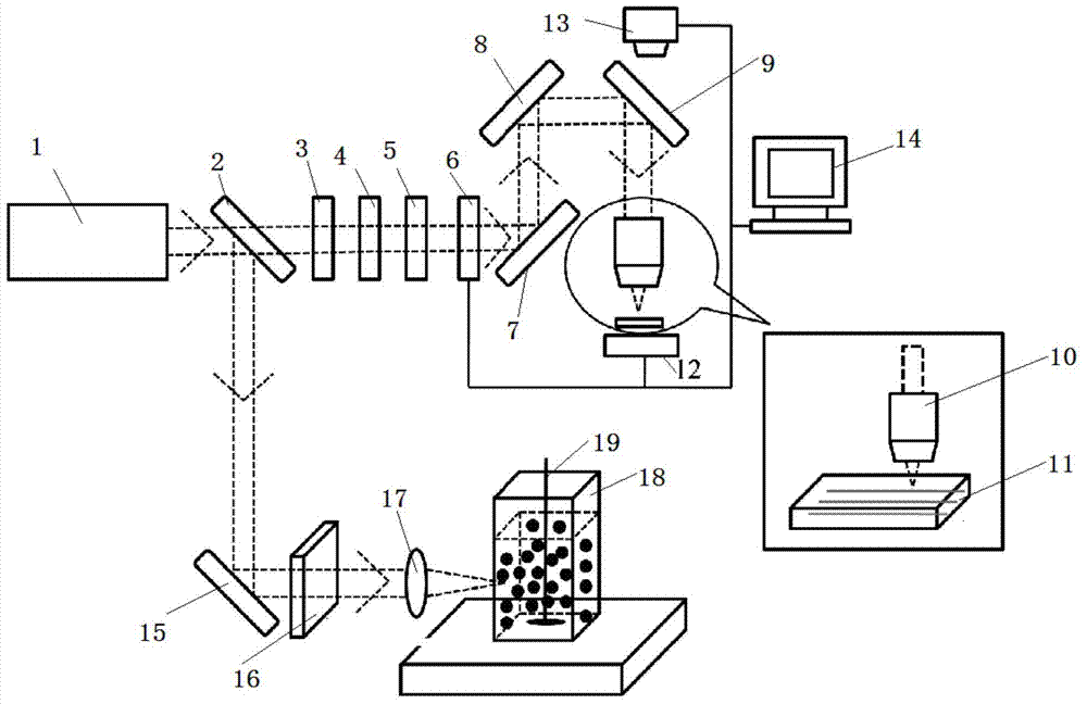
[0035] See figure 1 The structure shown, the process steps are as follows:

[0036] (1) Writing of microchannel pattern

[0037] Take a fused silica glass sample with a size of 10mm×10mm×1mm and six-sided polishing as the base material, clean the fused silica glass 11 and fix it on the electronically controlled translation stage 12, and the pulsed laser beam emitted by the femtosecond pulsed laser source 1 passes through the The beam splitter 2 with a split ratio of 1:9, the adjustable attenuation plate 3, the half-wave plate 4, the polarizer 5 and the mechanical shutter 6 are transmitted, and then pass through the first mirror 7, the second mirror 8 and the third mirror in turn 9 is reflected into the microscopic objective lens 10, irradiated to the surface of the fused silica glass 11 after being focused by the microscopic objective lens 10, and the fused silica glass 11 is irradiated controllably according to the designed micro-channel pattern, that is, the fused silica gl...

Embodiment 2

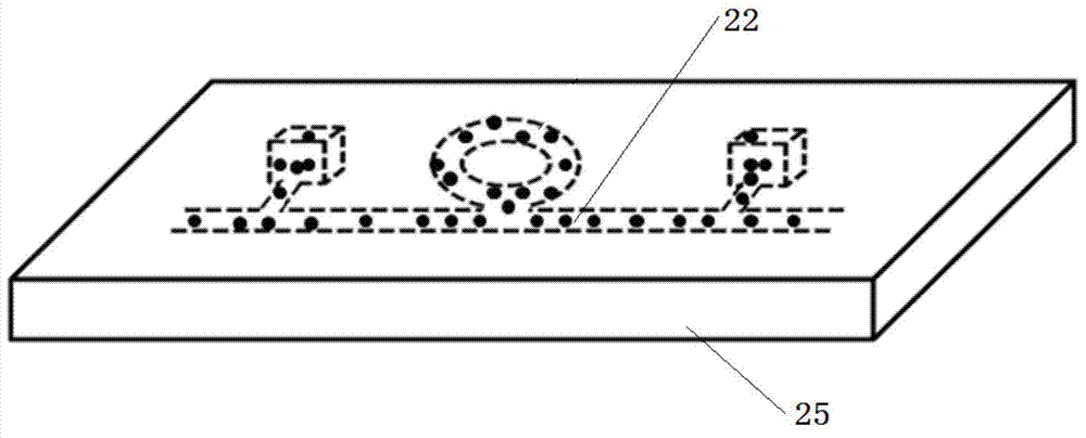
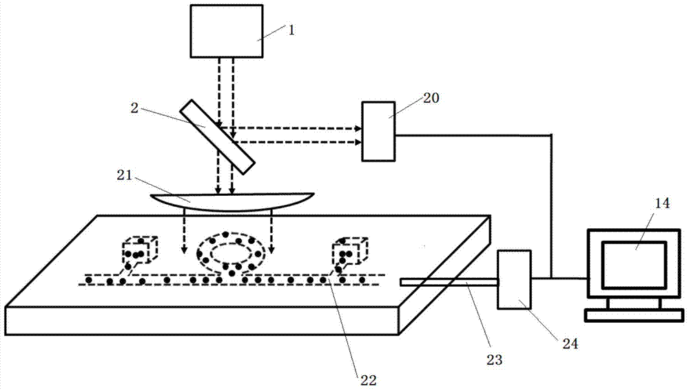
[0045] The difference between the method of preparing a microchannel-doped nanocrystal laser using a femtosecond pulsed laser described in this example and Example 1 is that the base material in step (1) is calcium fluoride crystal, and the hydrofluoric acid The mass concentration of mass concentration is 20%; The diameter size that obtains microchannel in the step (2) is 1 μm; The doping laser material used in the step (3) is doping YAG, and the crystal grain of gained doping nanocrystalline material is rod-shaped, The size of the rod-shaped grains is 20-100nm; the dispersion liquid described in the step (4) is distilled water, and the optical signal is coupled using an objective lens on the exit surface of the micro-channel, and the obtained micro-laser element 25 adopts polydimethylsilicon Oxane can be encapsulated.

Embodiment 3

[0047] The difference between the method of using femtosecond pulsed laser to prepare microchannel doped nanocrystal laser described in this embodiment and embodiment 1 is that the base material in step (1) is a silicon wafer, and the mass of the hydrofluoric acid Concentration is 5%; The diameter size that obtains microchannel in the step (2) is 15 μ m; The doping laser material used in the step (3) is doping ZnS, and the crystal grain of gained doping nanocrystalline material is rod shape, 20~ 100nm; the dispersion liquid in step (4) is ethanol, and the optical signal coupling on the exit surface of the micro-channel adopts waveguide coupling technology. The obtained micro-laser element 25 can be packaged with polymethacrylic acid.


PUM

PropertyMeasurementUnit
diameteraaaaaaaaaa
diameteraaaaaaaaaa
particle diameteraaaaaaaaaa

Abstract

The invention discloses a method for preparing a micro-channel doped nano-crystalline laser by using femtosecond pulse laser. The method comprises the following steps: (1) fixing a substrate material on an electrical control translation platform, focusing the femtosecond pulse laser through a microscope objective and irradiating to the surface or the interior of the substrate material, performing controllable irradiation according to a designed micro-channel pattern, and writing the designed micro-channel pattern in the substrate material; (2) preparing a micro-channel by using an auxiliary wet corrosion method; (3) crushing a blocky doped laser material and grinding into powder, dispersing into distilled water, and placing the distilled water in which the doped laser material is dispersed in a transparent container, focusing by using the femtosecond pulse laser under stirring and then directly performing irradiation ablation until the doped nano-crystalline material is obtained; (4) preparing the micro-channel doped nano-crystalline laser. The controllability of the output direction of the laser prepared by the method is high, and the laser can be used as a light source for an integrated optical chip.

Description

technical field [0001] The invention belongs to the technical field of integrated optical devices, and in particular relates to a method for preparing a microchannel-doped nanocrystal laser by using a femtosecond pulse laser. Background technique [0002] Micro-total analysis systems and lab-on-a-chip devices try to integrate multiple functional devices such as micro-fluidics, micro-optics, micro-electronics and micro-mechanics on the same chip that is only the size of a palm. The unparalleled advantages of the biochemical analysis system have set off a major revolution in the fields of biology, chemistry and medical science. [0003] To realize the integration of light source and microfluidic chip, several research groups have proposed and demonstrated microfluidic chip lasers based on different materials and structures. D.KilNNon[A microfluidic dye laserfabricated by nanoimprint lithography in a highly transparent and chemicallyresistant cyclo-olefin copolymer(COC)[J].Z M...

Claims


Application Information

Patent Timeline
Patent Type & Authority Patents(China)
IPC IPC(8): H01S5/30B81C1/00
Inventor 冯国英王树同杨超周寿桓
Owner SICHUAN UNIV
Features
  • R&D
  • Intellectual Property
  • Life Sciences
  • Materials
  • Tech Scout
  • Unparalleled Data Quality
  • Higher Quality Content
  • 60% Fewer Hallucinations
Learn More