
Surface enhanced Raman scattering sensor and preparation method thereof

A surface-enhanced Raman and sensor technology, which is applied in the directions of Raman scattering, material excitation analysis, etc., can solve the problem that it is difficult to obtain the SERS surface substrate with precise control of the degree of arraying, and achieve reduced production costs, simple preparation process, enhanced Effect of Raman scattering signal

Inactive Publication Date: 2015-04-29
SUZHOU INST OF NANO TECH & NANO BIONICS CHINESE ACEDEMY OF SCI
View PDF6 Cites 11 Cited by
  • Summary
  • Abstract
  • Description
  • Claims
  • Application Information

AI Technical Summary

Problems solved by technology

However, due to limiting factors such as substrate surface properties, processing difficulty, processing environmental conditions, and production costs, it is still difficult to obtain SERS surface substrates with precisely controlled nanostructure morphology, size, and arraying degree.

Method used


Image

  • Surface enhanced Raman scattering sensor and preparation method thereof
  • Surface enhanced Raman scattering sensor and preparation method thereof
  • Surface enhanced Raman scattering sensor and preparation method thereof

Examples


Embodiment 1

[0033] 4.89gAlCl 3 , 3.87gLiAlH 4 Dissolve in 30ml and 70ml of anisole respectively at -78°C under the protection of nitrogen. After the dissolution is complete, mix the two to form an aluminum hydride-anisole complex. Evaporate the solution to dryness and filter to obtain a white solid. The above solid was dissolved in 20ml of tetrahydrofuran solvent, and 1wt% surfactant was added at the same time to keep the ink stable for a long time. A conductive aluminum film layer with a thickness of 600 nm was printed on the ITO substrate by inkjet printing, and the active agent was ethylene glycol.

[0034] At a temperature of 60°C, with the ITO substrate printed with a conductive aluminum film layer as the anode and Pt as the cathode, the concentration of 15wt% H 2 SO 4 In the process, the anodic oxidation was carried out for 5h at a DC voltage of 40V. After the oxidation is completed, use 7% H 3 PO 4 and H at a mass concentration of 2% 2 CrO 4 Mix the solution to remove the a...

Embodiment 2

[0038] with AlH 3 {O(C 4 h 9 ) 2} solution as aluminum ink, with Ti(O-i-Pr) 4 As a catalyst, the catalyst was first coated on the substrate and preheated on a hot plate at 110°C for 60s, then the aluminum ink was printed on the substrate and reacted for 10 minutes to obtain a highly conductive aluminum layer with a thickness of 600nm. Among them, the preparation of aluminum ink is 1.33g of AlCl 3 , 1.11g of LiAlH 4 Dissolve in 50ml of butyl ether at -78°C under the protection of nitrogen. After the dissolution is complete, mix the two to form a complex of aluminum hydride-butyl ether. Evaporate the solution to dryness and filter to obtain a white solid. The above solid Dissolve in 20ml of tetrahydrofuran solvent, and add 1wt% surfactant at the same time to make aluminum ink; the substrate of this embodiment is glass.

[0039] At a temperature of 25°C, with a glass substrate printed with a conductive aluminum film layer as the anode and Pt as the cathode, in a concentrati...


PUM

PropertyMeasurementUnit
heightaaaaaaaaaa
diameteraaaaaaaaaa
thicknessaaaaaaaaaa

Abstract

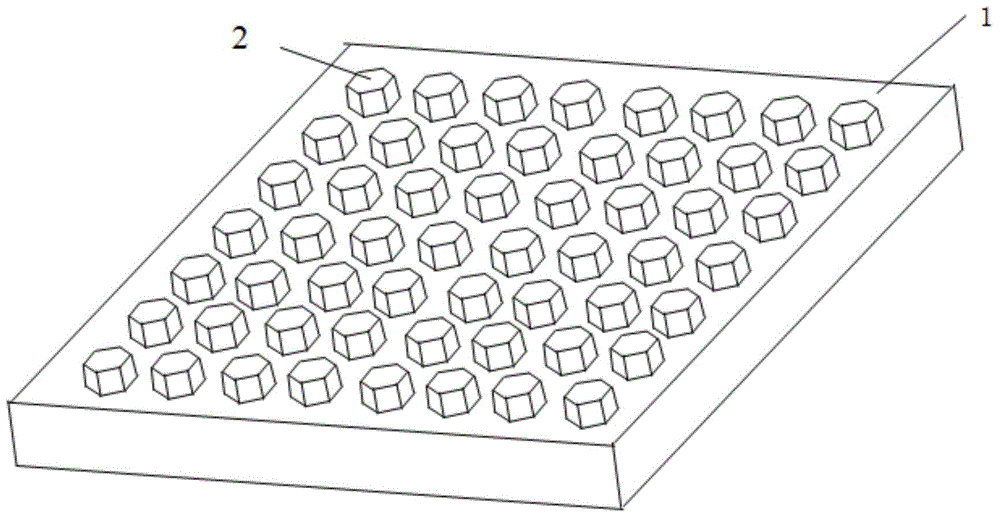
The inventing discloses a surface enhanced Raman scattering sensor. The surface enhanced Raman scattering sensor comprises a substrate and a metal nanometer pillar array arranged on the substrate, wherein the upper end surface of a metal nanometer pillar is planar, and the cross section of the metal nanometer pillar is hexagonal; the height of the metal nanometer pillar is 400-600nm and the diameter of the metal nanometer pillar is 100-200nm; and a distance between two adjacent metal nanometer pillars is 200-500nm. The invention also provides a preparation method of the surface enhanced Raman scattering sensor. According to the surface enhanced Raman scattering sensor, an anodic aluminum oxide template is used for assisting to obtain an array type nanometer pillar structure, a Raman scattering signal can be remarkably enhanced, and the surface enhanced Raman scattering sensor can be applied to the fields such as active biomacromolecules, narcotics, explosives, food sanitation, medical imaging, environment detection and the like; and besides, the preparation process of the sensor is simple, the conductive aluminum membrane layer is prepared by the printing process, the raw materials are saved, the production cost is reduced, the sensor is green and environmentally friendly, and the sensor is suitable for mass production.

Description

technical field [0001] The invention relates to the technical field of surface-enhanced Raman scattering chips, in particular to a surface-enhanced Raman scattering sensor and a preparation method thereof. Background technique [0002] Laser Raman spectroscopy has become one of the commonly used spectroscopic techniques for studying molecular structures in recent years. This is mainly due to the fact that infrared and Raman techniques are the only two characterization methods that can give molecular structure information among the existing spectroscopic techniques. However, the general Raman spectroscopy signal is relatively weak, the sensitivity is very low, and the light scattering signal is easily covered by fluorescence, which greatly reduces the practicability of Raman spectroscopy technology. It was not until 1977 that Van Duyne and Creighion found that the Raman signal of pyridine molecules adsorbed on a rough silver surface was about 10 times stronger than that of a...

Claims


Application Information

Patent Timeline
Patent Type & Authority Applications(China)
IPC IPC(8): G01N21/65
Inventor 潘革波赵宇肖燕刘永强吴浩迪
Owner SUZHOU INST OF NANO TECH & NANO BIONICS CHINESE ACEDEMY OF SCI
Learn More