Organic electroluminescent device and production method thereof

An electroluminescent device and electroluminescent technology, applied in the manufacturing of organic semiconductor devices, electro-solid devices, semiconductor/solid-state devices, etc., can solve the problems of poor stability, high driving voltage, low carrier mobility, etc.

Inactive Publication Date: 2015-05-20
OCEANS KING LIGHTING SCI&TECH CO LTD +2
View PDF0 Cites 10 Cited by
  • Summary
  • Abstract
  • Description
  • Claims
  • Application Information

AI Technical Summary

Problems solved by technology

[0003] Although organic electroluminescent devices have many advantages, compared with inorganic electroluminescent devices, organic electroluminescent devices have higher driving voltage and poor stability
The carrier mobility of the organic layer is low. Therefore, it is very important to reduce the driving voltage and improve the carrier injection efficiency and carrier mobility to improve the power conversion efficiency and life of the organic electroluminescent device. In order to solve these The problem is that the organic electroluminescent device uses an electron injection layer, but the electron injection efficiency of the organic electroluminescent device needs to be further improved

Method used


Image

  • Organic electroluminescent device and production method thereof
  • Organic electroluminescent device and production method thereof

Examples


Embodiment 1

[0035] A method for preparing an organic electroluminescent device, comprising the following steps:

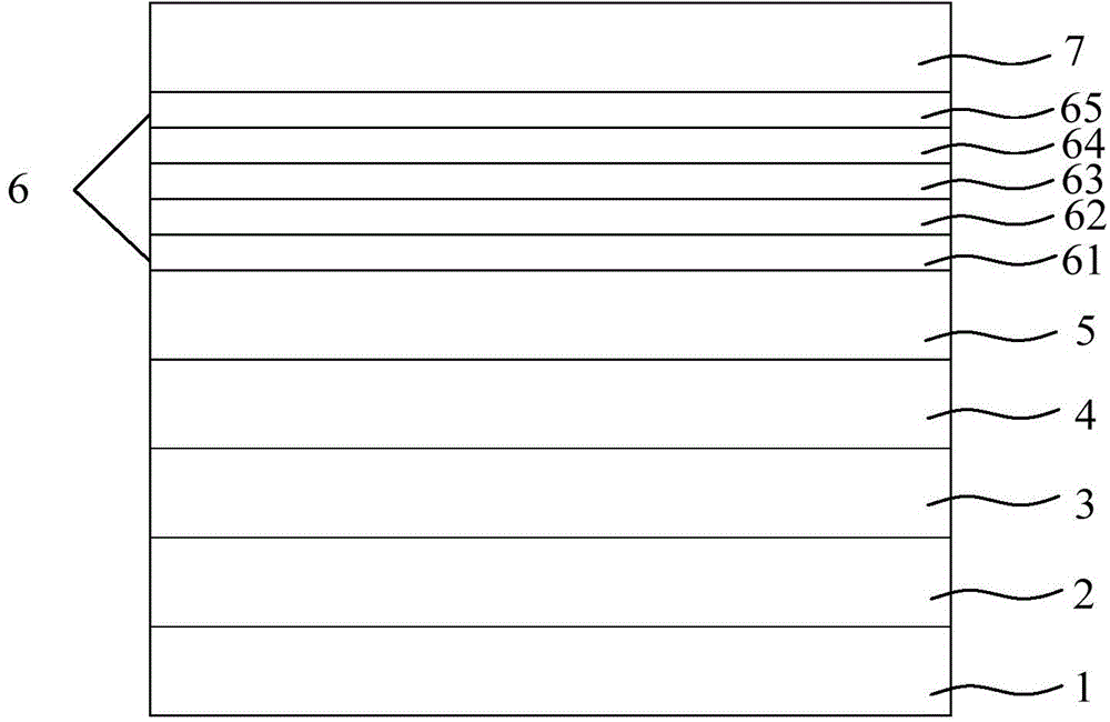
[0036] (1) Conductive anode 1 is made of indium tin oxide glass (ITO), and ultrasonicated with detergent, deionized water, acetone and ethanol for 5 minutes each to remove organic pollutants on the glass surface, cleaned and air-dried; The final ITO glass also needs surface activation treatment to increase the oxygen content on the ITO surface and improve the work function of the ITO surface; the thickness of the conductive anode 1 is 100nm; then the hole injection layer is prepared by vacuum evaporation on the conductive anode 1 2. Hole transport layer 3, light emitting layer 4 and electron transport layer 5;

[0037] The hole injection layer 2 is made of MoO 3 Hybrid material formed by doping N,N'-diphenyl-N,N'-bis(1-naphthyl)-1,1'-biphenyl-4,4'-diamine (NPB), MoO 3 The mass of the hole injection layer accounts for 30% of the mass of the hole injection layer, the thickness...

Embodiment 2

[0045] A method for preparing an organic electroluminescent device, comprising the following steps:

[0046] (1) Use indium tin oxide glass (ITO) as the conductive anode, and use detergent, deionized water, acetone and ethanol to ultrasonicate for 5 minutes each to remove organic pollutants on the glass surface, clean it and air dry it; The ITO glass also needs surface activation treatment to increase the oxygen content on the ITO surface and improve the work function of the ITO surface; the thickness of the conductive anode is 100nm; Transport layer, light emitting layer and electron transport layer;

[0047] The material of the hole injection layer is WO 3 Hybrid material formed by doping into 4,4',4''-tris(carbazol-9-yl)triphenylamine (TCTA), WO 3 The mass of the hole injection layer accounts for 25% of the mass of the hole injection layer, the thickness of the hole injection layer is 10nm, and the vacuum degree during evaporation is 5×10 -5 Pa, the evaporation rate is ...

Embodiment 3

[0055] A method for preparing an organic electroluminescent device, comprising the following steps:

[0056] (1) Use indium tin oxide glass (ITO) as the conductive anode, and use detergent, deionized water, acetone and ethanol to ultrasonicate for 5 minutes each to remove organic pollutants on the glass surface, clean it and air dry it; The ITO glass also needs surface activation treatment to increase the oxygen content on the ITO surface and improve the work function of the ITO surface; the thickness of the conductive anode is 100nm; Transport layer, light emitting layer and electron transport layer;

[0057] The material of the hole injection layer is V 2 o 5 Doped to 4,4'-bis(9-carbazole)biphenyl (CBP) to form a hybrid material, V 2 o 5 The mass of the hole injection layer accounts for 35% of the mass of the hole injection layer, the thickness of the hole injection layer is 15nm, and the vacuum degree during evaporation is 5×10 -5 Pa, the evaporation rate is

[0058...


PUM


Abstract

The invention discloses an organic electroluminescent device comprising a conductive anode, a hole injection layer, a hole transport layer, a luminescent layer, an electron transport layer, an electron injection layer and a cathode. The electron injection layer comprises a first doped layer, a second doped layer, a third doped layer, a fourth doped layer and a fifth doped layer stacked in order. The first doped layer, the second doped layer, the third doped layer, the fourth doped layer and the fifth doped layer are made of mixture made by doping a doped material to a base material; the doped material comprises a silver compound and an alkali metal compound; the silver compound is silver iodide, silver sulfide, silver chloride, silver fluoride or silver bromide; the alkali metal compound is lithium fluoride, lithium azide, lithium nitride, cesium fluoride, cesium azide or cesium nitride. The invention further provides a production method of the organic electroluminescent device.

Description

technical field [0001] The invention relates to the field of organic electroluminescence, in particular to an organic electroluminescence device and a preparation method thereof. Background technique [0002] Organic light-emitting devices (Organic light-emitting devices, referred to as OLEDs) is a multi-layer light-emitting device using organic light-emitting materials, including sequentially stacked anode layer, light-emitting layer and cathode. The luminescent principle of OLED is based on the action of an external electric field, electrons are injected from the cathode to the lowest unoccupied molecular orbital (LUMO) of organic matter, and holes are injected from the anode to the highest occupied orbital (HOMO) of organic matter. The light-emitting layers meet, recombine, and form excitons. The excitons migrate under the action of the electric field and transfer energy to the light-emitting material. The excited electrons transition from the ground state to the excited ...

Claims


Application Information

Patent Timeline
Patent Type & Authority Applications(China)
IPC IPC(8): H01L51/52H01L51/54H01L51/56
CPCH10K50/171H10K2102/00H10K2101/80H10K71/00
Inventor 周明杰钟铁涛王平张振华
Owner OCEANS KING LIGHTING SCI&TECH CO LTD
Why Eureka
Try Eureka