
Semiconductor resistance gas sensor and production method thereof

A gas sensor, resistive technology, applied in the direction of material resistance, etc., can solve the problems of unfavorable device repetitive production and industrial production application, excessive initial resistance value of the device, cumbersome device preparation method, etc., achieve good market application prospects, reduce The difficulty of detection and the effect of realizing mass production

Active Publication Date: 2015-06-17
HUAZHONG UNIV OF SCI & TECH
View PDF9 Cites 14 Cited by
  • Summary
  • Abstract
  • Description
  • Claims
  • Application Information

AI Technical Summary

Problems solved by technology

The study found that when SnO 2 When the ratio of ZnO to ZnO is 1:1, the maximum sensitivity of the material to methanol is about 9, but the preparation method of the device is too cumbersome, time-consuming and laborious, which is not conducive to the repetitive production of the device and industrial production application
Gupta et al. used laser deposition to prepare SnO 2 / CuO nanocomposite and studied its effect on H 2 The sensitivity of S gas is higher than that of pure-phase materials, but this preparation method requires high process precision and high sensor operating temperature, which is not conducive to composite materials taking advantage of nanomaterials in real devices.
Xue et al. successfully prepared the H 2 S gas heterojunction SnO 2 / CuO sensor, however, a high degree of sintering at 800 °C is required during the preparation process, resulting in additional energy loss
In 2014, Liu et al. synthesized nanoflower-like ZnO by a chemical water bath method, and obtained a NiO / ZnO heterostructure material with NiO nanoparticles on the surface after stirring and calcining the solution. The excessively high calcining temperature also has the problem of energy loss.
At the same time, in the field of sensors using nano-composite materials as gas-sensitive materials, there is also the problem of excessive initial resistance of the device, which puts forward higher requirements for the circuit structure and increases the difficulty of detection in actual use.

Method used


Image

  • Semiconductor resistance gas sensor and production method thereof

Examples


preparation example Construction

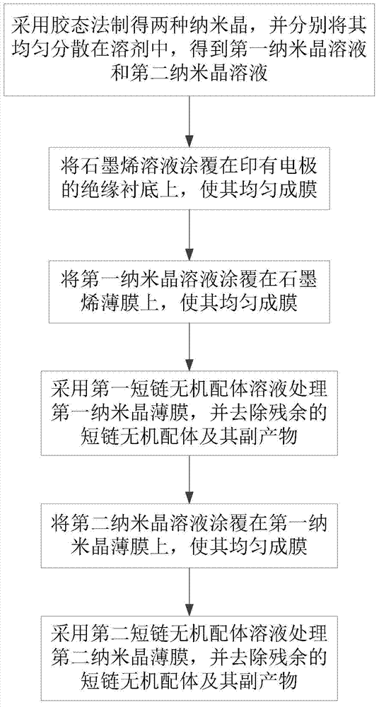
[0024] In the first embodiment of the present invention, the preparation method of the above-mentioned semiconductor resistive gas sensor comprises the following steps:

[0025] (1) Mix the precursor solutions of two kinds of nanocrystals, adopt a colloidal method to prepare a nanocrystal composite material, disperse it uniformly in a solvent, and mix graphene thereinto to obtain a composite solution;

[0026] (2) Coating the composite solution on an insulating substrate printed with electrodes to form a film uniformly;

[0027] Preferably, after the film is formed, the short-chain inorganic ligand solution is used to treat the film, and the remaining short-chain inorganic ligand and its by-products are removed;

[0028] (3) Repeat step (2) to obtain a gas-sensitive layer with a desired thickness, and complete the preparation of the gas sensor.

[0029] In the second embodiment of the present invention, the preparation method of the above-mentioned semiconductor resistive gas...

Embodiment 1

[0049] The preparation method of semiconductor resistive gas sensor comprises the steps:

[0050] (1) Preparation of SnO 2 Colloidal nanocrystal solution and CuO colloidal nanocrystal solution.

[0051] Among them, SnO 2 The preparation method of colloidal nanocrystal solution is specifically: under vacuum condition, 0.6g SnCl 4 ·5H 2 O, 20ml oleic acid (OA) and 2.5ml oleylamine (OLA) were mixed and stirred and heated to 80°C to prepare the precursor of tin oleate. After evacuating for 6 hours, the solution became clear. At this time, the heating and stirring were turned off, and nitrogen gas was passed into it to allow it to cool naturally. Inject 10ml of absolute ethanol into the above solution, take it out and transfer it to a stainless steel hydrothermal kettle and put it into an oven for hydrothermal reaction. Set the oven temperature to 180°C and keep it warm for 3 hours. After the hydrothermal reaction is over, take out the stainless steel hydrothermal kettle and p...

Embodiment 2

[0060] Steps (1) and (2) are the same as in Example 1, and steps (3) to (5) are specifically:

[0061] (3) The CuO colloidal nanocrystal solution is evenly dropped on the graphene film, spin-coated at a speed of 1300rpm for 30s, and repeated three times to make it evenly form a film;

[0062] Copper chloride (CuCl 2 ) with anhydrous methanol solution covering the entire nanocrystalline film, soaking for 45s and drying, repeating three times; soaking with anhydrous methanol for 15s and drying, repeating three times to remove residual CuCl 2 Particles and their reaction by-products.

[0063] (4) SnO 2 The colloidal nanocrystal solution is evenly dropped on the CuO colloidal nanocrystal film, spin-coated at a speed of 1300rpm for 30s, and repeated twice to form a uniform film;

[0064] Copper chloride (CuCl 2 ) with anhydrous methanol solution covering the entire nanocrystalline film, soaking for 45s and drying, repeating three times; soaking with anhydrous methanol for 15s a...


PUM


Abstract

The invention discloses a semiconductor resistance gas sensor and a production method thereof. The gas sensor comprises an insulation substrate, a signal electrode and a gas sensitive layer; and the gas sensitive layer is formed by a semiconductor nanocrystal composite material and graphene. A semiconductor nanocrystal solution is synthesized through a colloidal state technology, and can directly form a film at room temperature without high temperature treatment, so the energy consumption is small, agglomeration of nanoparticles is avoided, the large specific area advantages of the nanoparticles is maximally performed, gas adsorption is facilitated, and the sensitivity of the sensor is improved, thereby the sensor can be used to detect a target gas with a low concentration at a low work temperature and even normal temperature. The production method is simple, and can easily realize large scale batch production.

Description

technical field [0001] The invention belongs to the technical field of gas sensitive materials and components, and more specifically relates to a semiconductor resistive gas sensor and a preparation method thereof. Background technique [0002] The inherent sensitivity mechanism of the semiconductor resistive gas sensor determines that it is sensitive to a variety of gases and lacks selectivity, making it difficult to accurately identify the target gas, and it has certain requirements for the operating temperature, and the operating temperature affects the sensitivity of the gas-sensitive material to The reactivity of the gas, the state of chemically adsorbed oxygen on the surface, and the electron exchange process determine the sensitivity. With hydrogen sulfide (H 2 S) gas as an example, tin oxide (SnO 2 ) The optimal working temperature of the gas sensor is 150°C. Although the gas sensing characteristics can be improved to a certain extent by doping noble metal catalyst...

Claims


Application Information

Patent Timeline
IPC IPC(8): G01N27/12
Inventor 徐宋曼刘欢罗真李袁开宋志龙张文楷邵刚王阳
Owner HUAZHONG UNIV OF SCI & TECH
Learn More