Low-temperature in-situ growing method of semiconducting metal oxide with nano-structure as well as application

A nanostructure and in-situ growth technology, applied in the field of nanomaterials, can solve problems such as the inability of flexible organic and polymer material substrates to withstand high temperatures, difficulties in the development and application of flexible optoelectronic devices, and restrictions on the use of flexible polymer substrates. Effects of charge transfer, enhanced binding, and step-by-step convenience

Active Publication Date: 2015-07-29
ZHEJIANG UNIV
View PDF5 Cites 11 Cited by
  • Summary
  • Abstract
  • Description
  • Claims
  • Application Information

AI Technical Summary

Problems solved by technology

[0005] On the other hand, conventional methods for preparing semiconducting metal oxide nanomaterials usually require high-temperature treatment, while flexible organic and polymer material substrates are often unable to withstand high temperatures, which limits the use of flexible polymer substrates and hinders the development of flexible optoelectronic devices. and apply difficulties

Method used


Image

  • Low-temperature in-situ growing method of semiconducting metal oxide with nano-structure as well as application
  • Low-temperature in-situ growing method of semiconducting metal oxide with nano-structure as well as application
  • Low-temperature in-situ growing method of semiconducting metal oxide with nano-structure as well as application

Examples


Embodiment 1

[0034]The preparation method of the method of the present invention comprises the following steps:

[0035] 1. prepare the mixed solution of stannous chloride and polyvinyl butyral, i.e. spinning solution, the concentration of said stannous chloride is 85 mg / mL, and the concentration of polyvinyl butyral is 40 mg / mL; wherein Stannous chloride can be any metal salt that can be dissolved in the spinning solution solvent and has good compatibility with spinning aids, including but not limited to stannous chloride, tin tetrachloride, tetrabutyl titanate , tetraisopropyl titanium, zinc chloride, zinc acetate, ferric chloride, ferric nitrate; polyvinyl butyral can be any one or more oil-soluble polymers, including but not limited to polyvinyl butyral Aldehyde, polyvinylidene fluoride, polyvinyl chloride;

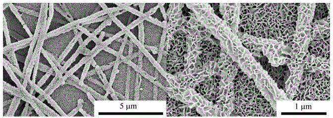
[0036] ② The electrospinning solution in step ① was deposited on the ceramic in the form of nanofibers under the electrospinning conditions of flow rate 0.2 mL / h; receiving di...

Embodiment 2

[0041] ① Prepare a mixed solution of zinc acetate and polyvinyl butyral, i.e. spinning solution, the concentration of zinc acetate is 10 mg / mL, and the concentration of polyvinyl butyral is 100 mg / mL;

[0042] ②The electrospinning solution in step ① was deposited in the form of nanofibers on the poly pairs under the electrospinning conditions of flow rate 0.1 mL / h; receiving distance 5 cm; spinning voltage 5 kV; receiving time 30 min. on an ethylene glycol phthalate base;

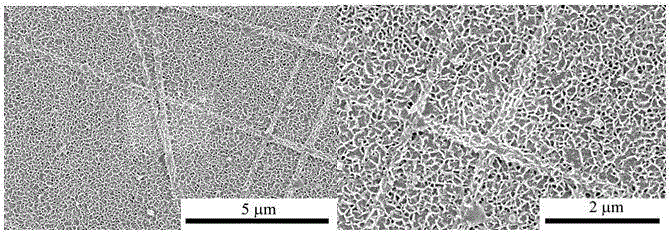
[0043] ③ drying the substrate deposited with nanofibers obtained in step ② and then hydrothermally treating it at 180° C. for 24 h to obtain a substrate with a semiconductor metal oxide nanostructure grown in situ, and the preparation method;

[0044] ④ In-situ polymerization and growth of polypyrrole on the substrate with the semiconductor metal oxide nanostructure obtained in step ③ to prepare a gas sensor.

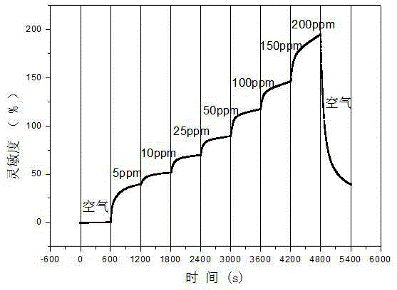
[0045] The resulting method exhibited a low resistance of less than 170 kΩ at lo...

Embodiment 3

[0047] 1. prepare the mixed solution of tin chloride and polyvinyl chloride, i.e. spinning solution, the concentration of said tin chloride is 300 mg / mL, and the concentration of polyvinyl chloride is 40 mg / mL;

[0048] ② The electrospinning solution in step ① was deposited in the form of nanofibers on the polystyrene under the electrospinning conditions of flow rate 1 mL / h; receiving distance 30 cm; spinning voltage 30 kV; receiving time 0.5 min. on a tetrafluoroethylene substrate;

[0049] ③ drying the substrate deposited with nanofibers obtained in step ② and then hydrothermally treating it at 120° C. for 6 h to obtain a substrate with a semiconductor metal oxide nanostructure grown in situ, and the preparation method;

[0050] ④ In-situ polymerization and growth of polypyrrole on the substrate with the semiconductor metal oxide nanostructure obtained in step ③ to prepare a gas sensor.

[0051] The resulting method has a low impedance of less than 200 kΩ at...


PUM


Abstract

The invention discloses a low-temperature in-situ growing method of a semiconducting metal oxide with a nano-structure as well as an application. According to the method, polymeric nanofibers containing an inorganic salt solution are deposited on a substrate with an electrospinning method, and then are subjected to hydro-thermal treatment, so that inorganic salt contained in the polymeric nanofibers is converted into the semiconducting metal oxide with the nano-structure in situ, and the semiconducting metal oxide is tightly combined with the substrate. The method has the advantages as follows: equipment is simple, steps are simple and convenient, the energy consumption is low, high-temperature thermal treatment is not required, a semiconducting metal oxide nano material is obtained on different substrates in situ at the relatively low temperature lower than 180 DEG C and the like; the method can be used for preparation of a flexible semiconducting metal oxide device with polymer as the substrate, further realizes good composition of the semiconducting metal oxide nano material and organic polymer conveniently, can be used for preparation of organic / semiconducting metal oxide nanocomposite materials and devices, and has a good application prospect in the field of nano photoelectric devices.

Description

technical field [0001] The invention relates to the field of nanomaterials, in particular to a method for realizing in-situ growth of nanostructured inorganic semiconductor metal oxides on different substrates by heat treatment at low temperature. Background technique [0002] Semiconductor metal oxides have great scientific research value and practical technical application value. More commonly used are SnO 2 , ZnO, TiO 2 , Fe 2 o 3 wait. Most of these semiconductor metal oxides are n-type multifunctional semiconductors with wide energy bands, which have excellent electrical properties, photocatalytic properties, electrochemical properties, photoelectric properties, gas sensing, humidity sensing, optical properties, etc. (L.b. Luo, F.x. Liang and J.s. Jie, Nanotechnology, 2011, 22, 485701; M. Batzill, K. Katsiev, J. M. Burst, U. Diebold, A. M. Chaka and B. Delley, Physical Review B, 2005, 72, 165414; H. Zhang, Q. He, X. Zhu, D. Pan, X. Deng and Z. Jiao, CrystEngComm, ...

Claims


Application Information

Patent Timeline
Patent Type & Authority Applications(China)
IPC IPC(8): G01N27/04
Inventor 李扬班会涛杨慕杰
Owner ZHEJIANG UNIV
Why Eureka
Try Eureka