Quick preparing method for large-area surface Raman spectrum enhancing monocrystalline silicon substrate

A surface-enhanced Raman and single crystal silicon technology, applied in Raman scattering, ion implantation plating, coating, etc., can solve the problems of low preparation efficiency, preparation cost and high environmental requirements, and achieve high structural reproducibility, The effect of short preparation cycle and high controllability

Inactive Publication Date: 2015-09-30
BEIJING UNIV OF TECH
View PDF4 Cites 14 Cited by
  • Summary
  • Abstract
  • Description
  • Claims
  • Application Information

AI Technical Summary

Problems solved by technology

At the same time, these methods also have the disadvantages of high preparation costs and environmental requirements, and low preparation efficiency.

Method used


Image

  • Quick preparing method for large-area surface Raman spectrum enhancing monocrystalline silicon substrate
  • Quick preparing method for large-area surface Raman spectrum enhancing monocrystalline silicon substrate
  • Quick preparing method for large-area surface Raman spectrum enhancing monocrystalline silicon substrate

Examples


Embodiment 1

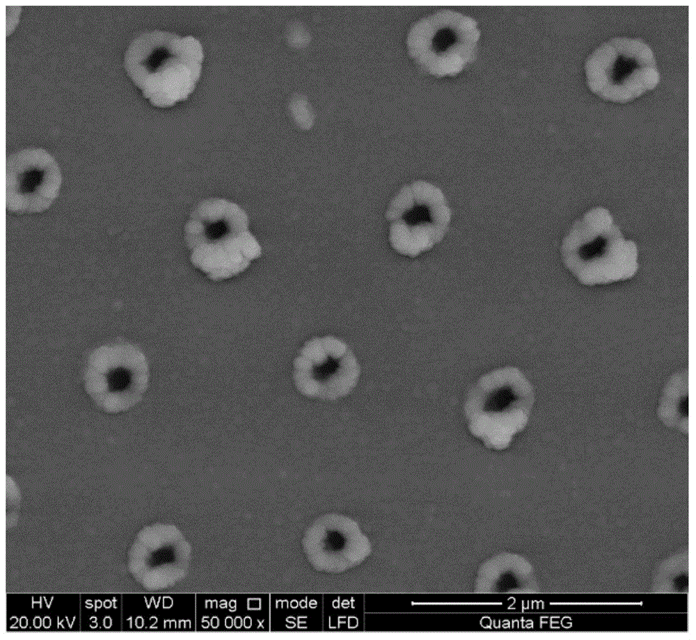
[0028] A single layer of SiO with hexagonal close-packed distribution was arranged on the surface of the cleaned single crystal silicon wafer sample by direct drop coating method 2 Microspheres, the size of the microspheres used is 1.5 μm; place the monocrystalline silicon sample on the target platform, adjust the optical path, and use an ultra-short pulse (10ps) laser with an ultraviolet wavelength to perform a positive defocus single line scan, and the scanning interval is the laser spot Size, repetition rate is 400kHz, scanning speed is 1200mm / s, power density is 5W / mm 2 ; Immerse the cleaned monocrystalline silicon sample in an aqueous sodium hydroxide solution containing ethanol, corrode it for 10 seconds in an environment with a water bath temperature of 75 ° C, take it out and rinse it with deionized water, and obtain a monocrystalline silicon wafer with a microstructure array, In the described aqueous solution, the mass percentage of sodium hydroxide is 10%, and the ma...

Embodiment 2

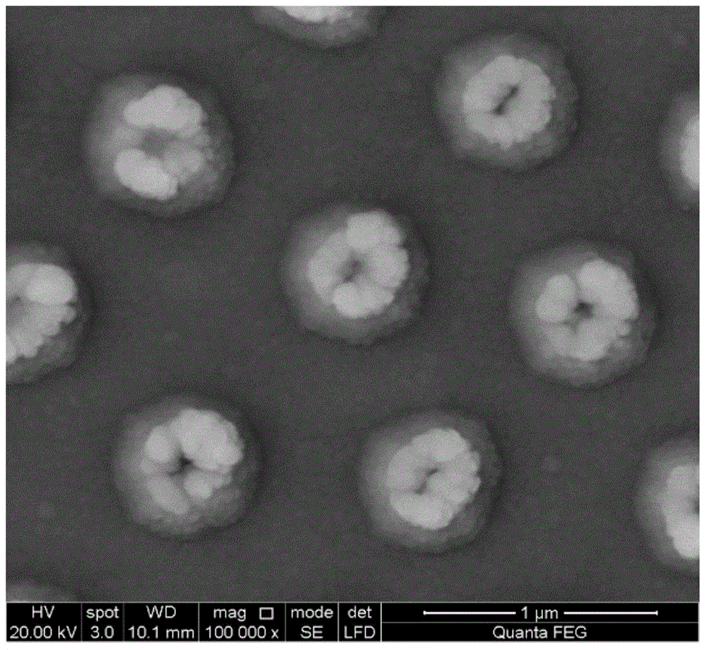
[0031] A single layer of SiO with hexagonal close-packed distribution was arranged on the surface of the cleaned single crystal silicon wafer sample by direct drop coating method 2 Microspheres, the size of the microspheres used is 1 μm; the single crystal silicon sample is placed on the target platform, the optical path is adjusted, and the ultrashort pulse (10ps) laser of ultraviolet wavelength is used for positive defocus single line scanning, and the scanning interval is the size of the laser spot , the repetition frequency is 200kHz, the scanning speed is 1000mm / s, and the power density is 20W / mm 2 ; Immerse the cleaned monocrystalline silicon sample in an aqueous sodium hydroxide solution containing ethanol, corrode it for 30 seconds in an environment with a water bath temperature of 75° C., take it out and rinse it with deionized water, and obtain a monocrystalline silicon wafer with a microstructure array, In the described aqueous solution, the mass percentage of sodiu...

Embodiment 3

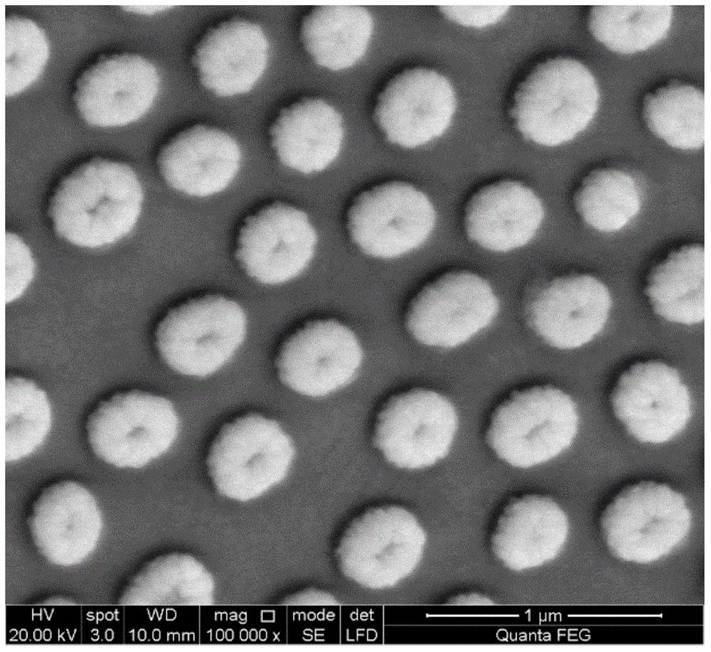
[0034] A single layer of SiO with hexagonal close-packed distribution was arranged on the surface of the cleaned single crystal silicon wafer sample by direct drop coating method 2 Microspheres, the size of the microspheres used is 0.5 μm; place the monocrystalline silicon sample on the target platform, adjust the optical path, and use an ultra-short pulse (10ps) laser with an ultraviolet wavelength to perform a single positive defocus line scan, and the scanning interval is the laser spot Size, repetition rate 200kHz, scanning speed 1200mm / s, power density 25W / mm 2 Immerse the cleaned monocrystalline silicon sample in an aqueous sodium hydroxide solution containing ethanol, corrode it for 30 seconds in an environment with a water bath temperature of 70° C., take it out and rinse it with deionized water, and obtain a monocrystalline silicon wafer with a microstructure array, In the described aqueous solution, the mass percentage of sodium hydroxide is 10%, and the mass percent...


PUM

PropertyMeasurementUnit
thicknessaaaaaaaaaa
thicknessaaaaaaaaaa

Abstract

The invention relates to a quick preparing method for a large-area surface Raman spectrum enhancing monocrystalline silicon substrate and belongs to the field of SERS substrate preparing. The quick preparing method comprises the steps that the surface of monocrystalline silicon is covered with a microballoon array which is periodically and densely arranged; microballoon left on the surface is removed through laser scanning or irradiating; the monocrystalline silicon is immersed into a sodium hydroxide water solution including alcohol, corrosion is carried out for 10-30 s in the environment with the water bath temperature ranging from 70 DEG C to 80 DEG C, the monocrystalline silicon is taken out and cleaned with deionized water, and the monocrystalline silicon with the microstructure array is obtained, wherein in the water solution, the sodium hydroxide accounts for 5%-10% by mass, and alcohol accounts for 8%-10% by mass; silver film deposition is carried out on the surface of the corroded monocrystalline silicon through magnetron sputtering, and the deposition thickness ranges from 50 nm to 200 nm. By means of the quick preparing method, the periodic and uniform microstructure array can be quickly, easily and conveniently prepared, and the performance of an SERS substrate can be controlled by controlling the morphology dimension feature of the microstructure array and the thickness of a silver film. Meanwhile, the method is high in reproducibility and low in cost, and prepared SERS substrate is stable in performance and capable of being repeatedly used.

Description

technical field [0001] The invention belongs to the field of surface Raman enhanced spectrum substrate preparation. Background technique [0002] Surface Raman-enhanced spectroscopy (SERS) has attracted extensive attention as a powerful detection and analysis tool since its discovery. Compared with ordinary Raman signals, in theory, when the target molecule to be detected is located between the gaps of metal nanoparticles, the enhancement factor of its SERS signal can reach 10. 14 times. This enhancement can make the originally weak Raman signal detectable, and even obtain a clear Raman fingerprint at the single-molecule level. The strong anti-interference ability of Raman scattering itself, combined with SERS technology, enables it to be applied in a variety of complex environments. The preparation of SERS substrates is usually by depositing metal nanoparticles on solid substrates by chemical synthesis or self-assembly effect, and this method can obtain a strong enhancem...

Claims


Application Information

Patent Timeline
Patent Type & Authority Applications(China)
IPC IPC(8): G01N21/65C23C14/35C23C14/16
Inventor 季凌飞林真源吴燕吕晓占闫胤洲蒋毅坚
Owner BEIJING UNIV OF TECH
Why Eureka
Try Eureka