Optical waveguide sensing chip, preparation method thereof, and use

A sensor chip and optical waveguide technology, applied in scanning probe technology, instruments, etc., can solve the problems of poor acid-base stability, difficult synthesis, and complicated preparation process of alumina

Inactive Publication Date: 2015-10-21
SHENZHEN GRADUATE SCHOOL TSINGHUA UNIV
View PDF5 Cites 3 Cited by
  • Summary
  • Abstract
  • Description
  • Claims
  • Application Information

AI Technical Summary

Problems solved by technology

[0003] At present, the relatively mature nanostructure film materials used in optical waveguide sensors mainly include porous anodized aluminum oxide films, porous titanium dioxide films, mesoporous silica films, hydrogel films, and some materials filled with anodized aluminum oxide as templates. Nano-column (tube) array film, etc. However, the nano-structure film materials used in optical waveguide sensors prepared in the past have certain defects, such as poor acid-bas

Method used


Image

  • Optical waveguide sensing chip, preparation method thereof, and use
  • Optical waveguide sensing chip, preparation method thereof, and use
  • Optical waveguide sensing chip, preparation method thereof, and use

Examples


preparation example Construction

[0031] In some embodiments, a method for preparing an optical waveguide sensor chip based on a nanopillar array structure, the method includes the following steps:

[0032] (1) the gold film substrate is immersed in the organic solution of mercaptosilane to process;

[0033] (2) process the gold film substrate after processing in step (1) with acid solution;

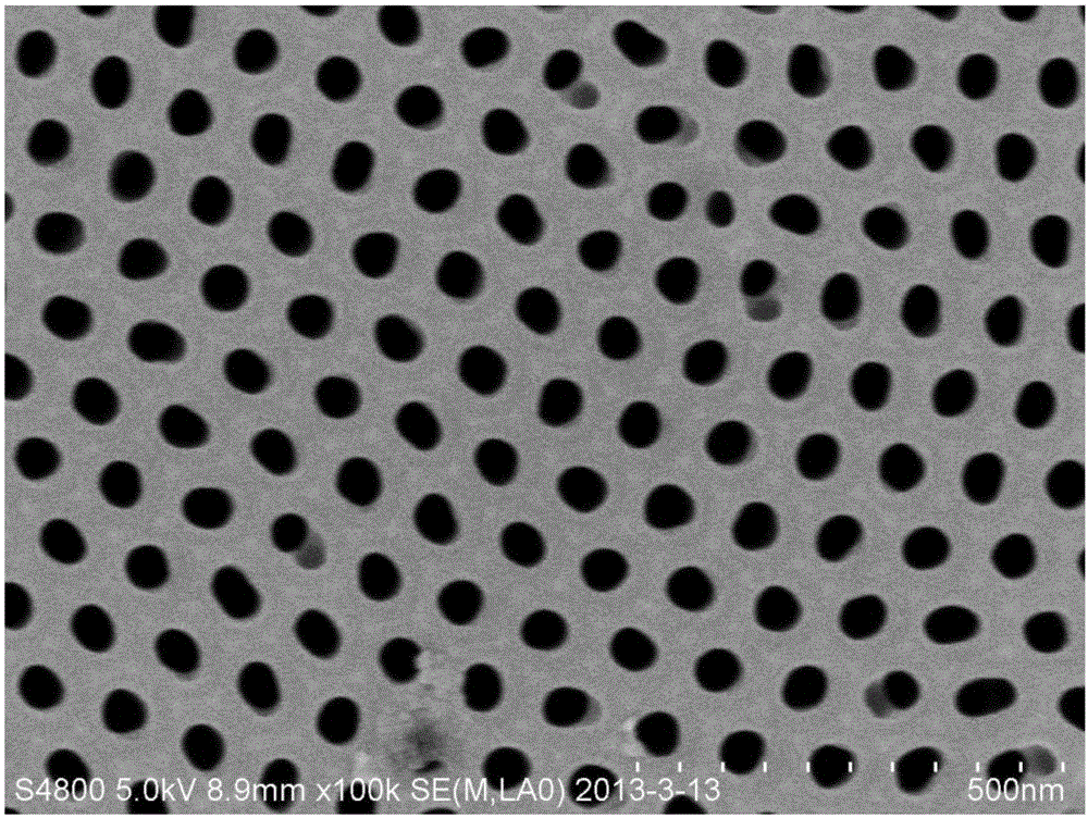
[0034] (3) the porous anodic aluminum oxide film is pasted on the gold film surface after step (2) processing;

[0035] (4) the permeable porous aluminum oxide film pasted on the surface of the gold film obtained through step (3) is immersed in solution for a period of time;

[0036] (5) stirring the sample obtained through step (4) with an acidic organic solution;

[0037] (6) Treat the sample treated in step (5) with an acid solution.

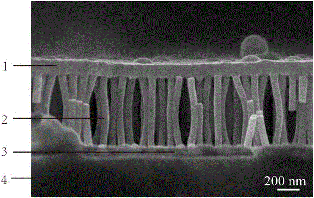
[0038] According to an embodiment of the present invention, in step (1), the gold film is a gold layer with a thickness of 40-50nm, preferably 40-45nm, coated on the surface of the...

Embodiment 1

[0051] This specific example is used to illustrate the preparation of an optical waveguide sensor chip of a mesoporous silica nano-column array film by using the method of the embodiment of the present invention.

[0052] (1) Preparation of gold film: immerse the K9 glass sheet in H with a volume ratio of 1:2 2 o 2 (mass fraction is 30%) and H 2 SO 4 (mass fraction is 98%) in the mixed solution, stand for 2 hours, then rinse with a large amount of deionized water, blow dry with nitrogen. The cleaned K9 glass sheet was sputtered with a layer of 2nm thick chromium as an adhesion layer by magnetron sputtering method, and then a layer of 40nm thick gold was sputtered, which is the gold substrate used in this embodiment.

[0053] (2) Ethanol solution treatment of gold film substrate with mercaptosilane: prepare 20 mmol / L (3-mercaptopropyl)trimethoxysilane solution with ethanol. Immerse the gold film substrate obtained in step (1) in the above solution for 8 hours.

[0054] (3)...


PUM

PropertyMeasurementUnit
Thicknessaaaaaaaaaa
Concentrationaaaaaaaaaa

Abstract

A preparation method of an optical waveguide sensing chip comprises immersing a gold film substrate in an organic solution of mercapto silance to be processed, processing the processed gold film substrate by utilizing an acid solution, pasting a porous anodic aluminum oxide film to a surface of a gold film, immersing the aluminum oxide film pasted to the surface of the gold film in a mixed solution of cetyltrimethyl ammonium bromide (CTAB), water, ethyl alcohol, concentrated ammonia liquor and tetraethyl orthosilicate (TEOS) and standing for a period of time, and processing the processed product by utilizing an acid solution to remove the porous aluminum oxide film. The invention discloses the optical waveguide sensing chip and use of the optical waveguide sensing chip for non-labeled optical biological detection or heavy metal ion detection. The optical waveguide sensing chip is an optical waveguide sensing chip prepared by the method based on a nano-column array film. The optical waveguide sensing chip can be used to perform the high-sensitivity non-labeled optical biological detection or the high-sensitivity heavy metal ion detection.

Description

technical field [0001] The invention relates to a preparation method of an optical waveguide sensor chip, an optical waveguide sensor chip prepared by the method and its application, in particular to an optical waveguide sensor chip with a gold film as the base and a mesoporous silica nano-column array structure. A preparation method of a waveguide sensor chip, and the application of the chip in the detection of small molecules and heavy metal ions. Background technique [0002] Optical biosensors have the advantages of high detection sensitivity, large dynamic detection range, and low detection limit, and have been applied in many fields, including biomedical research, environmental monitoring, and medical diagnosis. Among optical biosensors, optical biosensors based on detection of refractive index changes are widely used. Among them, the surface plasmon resonance sensor is the most widely studied and applied in the non-labeled optical biosensor, and its sensitivity to th...

Claims


Application Information

Patent Timeline
IPC IPC(8): G01Q30/02
Inventor 孙树清丁宇张亚飞
Owner SHENZHEN GRADUATE SCHOOL TSINGHUA UNIV
Why Eureka
Try Eureka